ASIA ELECTRONICS INDUSTRYYOUR WINDOW TO SMART MANUFACTURING
OKI, Shin-Etsu Technology Enables Vertical GaN Devices
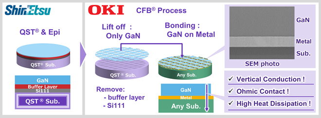
OKI Electric Co., Ltd., in collaboration with Shin-Etsu Chemical Co., Ltd., has developed a lifting off/bonding technology of GaN layer on QST substrates.
Specifically, the new technology uses OKI’s CFB (crystal film bonding) technology (*1) to lift off only the GaN (gallium nitride) functional layer from Shin-Etsu Chemical’s uniquely improved QST® (Qromis Substrate Technology) substrate (*2) and bond it to a different material substrate. This technology enables the vertical conduction of GaN. Moreover, it will contribute to the realization and commercialization of vertical GaN power devices capable of controlling large currents.
Further, the two companies will continue to work to develop vertical GaN power devices that can be implemented in society. They aim to partner with companies that manufacture these devices.
GaN devices are attracting attention as next-generation devices that combine high device characteristics with low power consumption. Among them are power devices that require high breakdown voltages of 1,800V or more, high-frequency devices for Beyond5G, and high-brightness micro-LED displays. Mainly, significant demand growth is seen for vertical GaN as devices that can improve the basic performance of electric vehicles. Specifically, GaN power devices endow EV with extended driving ranges and shortened power supply times. However, two major challenges hinder the social implementation of vertical GaN power devices. First, the diameter of the wafers must be increased to improve productivity. Second, vertical conductivity must be realized to enable large current control.
The coefficient of thermal expansion of Shin-Etsu Chemical’s QST substrate is equivalent to that of GaN. It can suppress warpage and cracking. This characteristic enables the crystal growth of thick GaN films with high breakdown voltages even on wafers larger than 8 inches. Thus, it enables the production of wafers with larger diameters.
On the other hand, OKI’s CFB technology can lift off only the GaN functional layer from the QST substrate while maintaining high device characteristics. The insulating buffer layer required for GaN crystal growth can be removed and bonded to various substrates via metal electrodes that allow ohmic contact (*3). Bonding of these functional layers to a conductive substrate with high heat dissipation will enable both high heat dissipation and vertical conductivity. Through this, the combined technologies of Shin-Etsu Chemical and OKI solve the above two major challenges, paving the way for the social implementation of vertical GaN power devices.
In the future, the two companies will contribute to the realization and widespread use of vertical GaN power devices. Specifically, Shin-Etsu Chemical will provide QST substrates or GaN grown QST substrates to companies manufacturing GaN devices. At the same time, OKI will provide CFB technology through partnering and licensing. Furthermore, OKI hopes to use CFB technology to provide added value to semiconductor devices that go beyond the framework of single materials and help realize the company’s key message of “Delivering OK! to your life”.
Explanation of terminology
*1: CFB (crystal film bonding) technology
A technology to lift off crystal films from growing substrates, and bond it to a different material substrate.
*2: QST (Qromis Substrate Technology) substrate
A composite material substrate developed by Qromis, Inc. (Head Office: California; CEO Cem Basceri) exclusively for GaN growth. In 2019, Shin-Etsu Chemical got the license.
*3: Ohmic contact
An electrical bonding with a linear current-voltage curve according to Ohm’s law.
- Share: