ASIA ELECTRONICS INDUSTRYYOUR WINDOW TO SMART MANUFACTURING
New Nikon Immersion Scanner Suits Cutting-Edge ICs
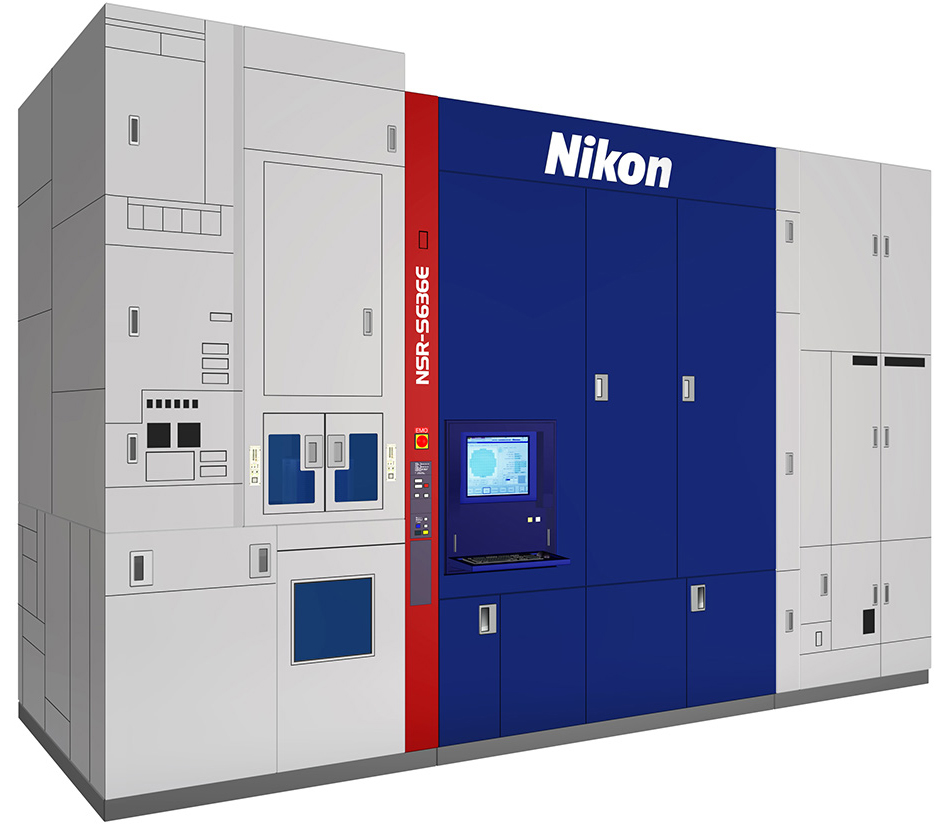
Nikon Corporation has launched the NSR-S636E ArF immersion scanner featuring the highest productivity of any lithography system across its history. Because of this NSR-S636E, suits critical layers and delivers superior overlay accuracy and ultra-high throughput. Mainly, NSR-S636E is the optimum patterning solution for the many diverse structures used in cutting-edge semiconductors, including 3D devices. The company plans to launch sales of the product in January 2024.
As the digital transformation accelerates, high-performance semiconductors that can process and transmit larger amounts of data more quickly are becoming increasingly critical. The key enablers in technology innovation for leading-edge semiconductor performance are circuit pattern miniaturization and 3D semiconductor device structures.
Specifically, ArF immersion scanners are essential for both of these manufacturing processes. When compared to conventional semiconductors, wafer warpage and distortions are more likely to occur during 3D semiconductor manufacturing. As a result, this necessitates even more advanced scanner correction and compensation capabilities than ever before.
Moreover, NSR-S636E utilizes an enhanced iAS*1 that performs sophisticated wafer multipoint measurement before exposure. Also, this innovative system delivers next-level overlay accuracy using high-precision measurement and extensive wafer warpage and distortion correction capabilities. It achieves all these while maintaining maximum scanner throughput. Also, the overall scanner output is 10 to 15% higher*2 than current generation systems. Accordingly, this results in optimized efficiency in cutting-edge semiconductor device production. Nikon continues to provide invaluable solutions like NSR-S636E for leading IC production and supporting the development of the digital society.
Key Benefits
Excellent performance across diverse production processes including 3D-ICs where wafer deformation can easily occur
Enhanced accuracy of the inline alignment station (iAS) that performs wafer multipoint measurement before exposure enables heightened accuracy in measuring deformations such as wafer warping and distortion. Advanced measurement and compensation capabilities improve process robustness and provide superior overlay performance, without impacting productivity. These innovations are invaluable to diverse manufacturing processes including 3D-ICs that require ultra-high overlay accuracy and will continue to be developed to achieve unprecedented semiconductor performance.
Highest productivity among all Nikon semiconductor lithography systems
Through comprehensive improvements in throughput and daily productivity optimization, the NSR-S636E ArF immersion scanner boosts overall output by 10-15% compared to current models. This is the highest level of productivity across the entire history of Nikon semiconductor lithography systems.
Nikon commits to continuing to push the limits of photolithography through industry-leading solutions like the NSR-S636E to support its customers’ manufacturing objectives for many years to come.
*1 inline Alignment Station – this system measures wafers with high speed and accuracy and enables grid error correction without reducing exposure system throughput.
*2 This can vary depending on usage conditions and other factors.
- Share: