ASIA ELECTRONICS INDUSTRYYOUR WINDOW TO SMART MANUFACTURING
Nikon Releases New ArF Immersion Scanner
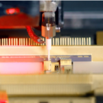
Nikon Corporation releases NSR-S625E, an ArF immersion scanner optimized especially for middle critical layers. NSR-S625E features the highest productivity in the history of Nikon’s lithography systems, thanks to its enhanced throughput and operational stability. Mainly, it will contribute to the efficient production of various semiconductor devices.
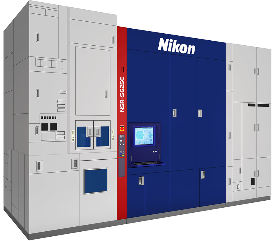
Specifically, the NSR-S625E ArF immersion scanner features a resolution of ≤ 38nm and a numerical aperture of 1.35. A 193nm wavelength ArF excimer laser is the source of exposure light. Moreover, it has a reduction ratio of 1:4 and a maximum exposure field of 26×33mm. The new ArF scanner has a throughput of ≥ 280 wafers/hour (96 shots). In terms of single machine overlay (NSR-S625E #1 to NSR-S625E #1), accuracy is ≤ 1.7nm, while mix and match overlay (NSR-S625E #1 to NSR-S625E #2) is ≤ 2.5nm.
Development Background
Generally, the demand for semiconductor devices widely varies along with the diversification of their applications. The requirement for lithography systems, which are essential for semiconductor device manufacturing, is becoming more complex and sophisticated.
Nikon has been providing the best solutions together with its customers. To satisfy the diverse customer needs more than ever and to expand its product lineup, Nikon has developed a new lithography system. The new NSR-S625E is the successor to the NSR-S622D, which is in the commercial market for over 10 years. Also, with a throughput approximately 1.3 times that of the NSR-S622D, NSR-S625E offers significantly improved operational stability. Additionally, it incorporates an iAS*1, contributing to enhanced production efficiency for a wide range of semiconductor devices.
Nikon will continue to contribute to the manufacturing of high-value-added semiconductor devices by providing lithography systems that best suit customer needs.
*1inline Alignment Station: The alignment station performs high-speed, ultra-precise measurement of all wafers, and then corrects problematic grid errors without reducing the throughput of the lithography system.
- Share: