ASIA ELECTRONICS INDUSTRYYOUR WINDOW TO SMART MANUFACTURING
New Coupling Device by Murata Fits Next-Gen Wi-Fi
Murata Manufacturing Co., Ltd. has announced its new Parasitic Element Coupling Device. Specifically, this is a state-of-the-art solution that improves antenna efficiency by magnetically coupling the parasitic element with the antenna. Also, this is the first solution designed for Wi-Fi 6E and Wi-Fi 7 products. For designers of smartphones, tablets, network routers, game consoles, and other compact electronics, it enables them to build more efficient antennas. This is a key requirement for many modern space-constrained devices.

To develop products conforming to Wi-Fi 6E and Wi-Fi 7 standards, which utilize high-speed wireless communication, multiple high-performance antennas must be installed in electronic devices to improve communication speed and quality. However, as the dimensions of heatsinks and batteries expand and as processors become more advanced, the available space for mounting antennas tends to decrease.
Consequently, there is a need for smaller antennas. But there is a technical limitation, in that the efficiency of wide-band antennas decreases when they are miniaturized. Therefore, designers need a solution that achieves both miniaturization and high performance.
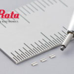
The solution from Murata is a parasitic element coupling device. It is made with its multilayer technology as a four-terminal surface-mount component of just 1.0 × 0.5 × 0.35mm.
Also, this parasitic element coupling device connects the feeding antenna* to its parasitic elements more effectively than is possible through free space. It acts as a tiny coupling device whose compact size enables strong coupling performance without the use of magnetic materials, which would be inappropriate at the targeted operating frequencies.
One side of the coupling device is connected, at very low insertion loss, between a device’s RF circuitry and its main antenna. Meanwhile, the other side is connected between the ground and the parasitic element. The resultant, more direct coupling enables the resonance characteristics of the parasitic element to be added to those of the feeding antenna. As a result, it enables more efficient operation across a broader frequency range or on multiple discrete bands.
The device helps to combat that when an antenna is made smaller, the coupling between it and the parasitic elements is reduced, while the coupling between the parasitic elements and the ground is increased. By sustaining the coupling between the feeding antenna and parasitic element, parasitic element coupling device enables designers to use miniaturized antenna design methods without impacting the communication band of efficiency.
The feeding antenna can cause an impedance mismatch when used over a wide band, leading to a degradation in wireless performance. In addition, when an antenna with a mismatched impedance is connected to a communication circuit using a long cable, the long cable can promote the impedance mismatch, causing larger insertion loss than expected and significantly reducing wireless communication performance. By using the device, engineers can improve antenna matching and reduce performance degradation in wireless communications even when using long cables.
*An antenna connected to RF module with cable, etc.
- Share: