ASIA ELECTRONICS INDUSTRYYOUR WINDOW TO SMART MANUFACTURING
FUJIFILM Rolls New Facility for CMP Slurry in Japan
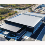
FUJIFILM Corporation announces that its new production facility for Chemical Mechanical Polishing (CMP) slurries at its Kumamoto site has begun full-scale operation. CMP slurries are basic materials used in semiconductor manufacturing process.
FUJIFILM Electronic Materials Co., Ltd. (FFEM), the core company that leads Fujifilm’s Electronic Materials business installed the new facility. It involves an investment of approximately 2 billion yen at the Kyushu site of FUJIFILM Material Manufacturing Co., Ltd. (FFMT Kyushu), a display materials production site located in Kumamoto Prefecture, Japan.
Fujifilm has launched FFMT Kyushu as its Kumamoto base for semiconductor materials. It produces display and semiconductor materials to ensure supply stability. This is Fujifilm’s first production facility for CMP slurries in Japan.

To Support High-speed Communication in 5G/6G
Demand for semiconductors is expected to increase and performance is projected to advance against the backdrop of faster and higher communication speeds with 5G/6G, the spread of automated driving, AI and the metaverse. Under these circumstances, it is increasingly important to ensure a stable supply of higher quality and higher performance semiconductor materials used in the semiconductor manufacturing process.
CMP slurries are polishers for evenly levelling semiconductor surface, which contains a mixture of wires and insulation films of varying hardness. The market is growing at a rate of 10% per annum*. Fujifilm has CMP slurries production facilities in Arizona, USA, in Cheonan, South Korea, and in Hsinchu, Taiwan. It is expanding CMP slurries sales by continuing to meet customers’ high demands for stable supply and quality.
FFEM has introduced and started the full-scale operation of the state-of-the-art production facility and quality assessment equipment for CMP slurries at FFMT Kyushu, a main production base for display materials. The company combines the new facility/equipment with the human resources and manufacturing expertise of FFMT Kyushu to produce high-quality and high-performance CMP slurries. It is known to meet the high-quality demands of customers for display materials.
By producing CMP slurries domestically in Japan, Fujifilm is now able to supply CMP slurries to its domestic customers in a timely manner. Fujifilm now has a total of four sites worldwide with enhanced production capacity to meet the growing global market.
In addition, FFMT Kyushu plans to start operation of a state-of-the-art facility to produce color filter materials for image sensors in the spring of 2025, expanding its semiconductor materials production lineup.
Fujifilm offers process chemicals used in the pre- and post-processes of semiconductor manufacturing. Among them include photoresists, photolithography-related materials, CMP slurries, post-CMP cleaners, thin-film formation materials and polyimides, as well as Wave Control Mosaic (WCM) materials such as color filter materials for image sensors.
Leveraging the strength of a broad product lineup and global stable supply structure as well as its advanced R&D capabilities and solid trusting relationships with customers, the company is striving to accelerate business growth. Specifically, it aims to achieve 500 billion yen in global revenues of Electronic Materials business by FY2030. Fujifilm will continue to contribute to the development of the semiconductor industry through the development and supply of cutting-edge semiconductor materials.
* According to Fujifilm data
- Share: