ASIA ELECTRONICS INDUSTRYYOUR WINDOW TO SMART MANUFACTURING
FUJIFILM to Build New Materials Factory in Taiwan
FUJIFILM Corporation has announced that it will build a new factory for cutting-edge semiconductor materials in Taiwan. This strategic decision targets to expand further its electronic materials business. To achieve this, FUJIFILM Electronic Materials Taiwan Co., Ltd. will acquire land in Hsinchu City and build a new factory for producing CMP slurries*1 and photolithography-related materials*2. FUJIFILM Electronic Materials Taiwan is the company’s semiconductor materials subsidiary in Taiwan and is due to go operational in the spring of 2026.
Additionally, the company will expand its existing factory, the Third Taiwan Factory, in Tainan City. The company will include CMP slurry manufacturing capability in the new building under construction. Specifically, it will commence operation in the spring of 2024.
The total amount of capital investment, combining the construction of the new factory and facility reinforcement of the existing factory, comes to approximately 15 billion yen*3 (US$107 million).

Reinforced Operation
Mainly, the new factory in Hsinchu City for cutting-edge semiconductor materials will expand the product supply capacity of FUJIFILM Electronic Materials Taiwan to cater to the fast-growing semiconductor market in Taiwan. Accordingly, the factory will feature the latest manufacturing facilities and quality assessment equipment. Thus, it can strengthen its production capabilities and technical support structures for CMP slurries and photolithography-related materials.
Additionally, a product warehouse is being established in order to put up a supply structure capable of responding to customer requests in detail. Installed photovoltaic solar panels will reduce the factory’s environmental impact. The office function of the adjacent First and Second Taiwan Factories will be integrated into the new facility for reinforced intra-factory collaboration. For the expansion of production capabilities at the new and existing factories, the company plans to create about 50 new jobs.
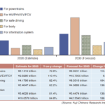
The semiconductors segment is expected to achieve approximately 10% market growth annually*4 and see further performance advancement against the backdrop of 5G/6G-triggered communications advancement in speed and capacity, proliferation of self-driving vehicles and spread of Metaverse.
FUJIFIL offers process chemicals used in pre- to post-processes in semiconductor manufacturing. Among them include photoresists*5, photolithography-related materials, CMP slurries, post-CMP cleaners*6, thin-film formation materials*7 and polyimides,*8. It also includes Wave Control Mosaic (WCM)*9 materials such as color filter materials for image sensors. In addition to the broad product lineup, the company is tapping into its stable global supply structure, advanced R&D capability, and solid trusting ties with clients to expand the business further.
Currently, it is undertaking active capital investments in the global markets. This includes the introduction of CMP slurry production facilities in Japan and the reinforcement of polyimide manufacturing facilities in Belgium. This way, it will build up the ability to cater to surging demand for semiconductors.
FUJIFILM will infuse capital investments and other efforts to accelerate business growth. Accordingly, it aims to achieve 500 billion yen (US$3.56 billion) in revenues in its global electronic materials business by FY2030. The company continues to contribute to the development of the semiconductor industry through the development and supply of cutting-edge semiconductor materials.
*1 Chemical Mechanical Polishing (CMP) slurry is a polisher for evenly leveling semiconductor surface, which contains a mixture of wires and insulation films of varying hardness.
*2 Development solutions, cleaners and other materials used in the photolithography process of semiconductor manufacturing
*3 Including the construction cost of the new building in progress
*4 According to Fujifilm data
*5 Material used to coat wafer substrate when circuit patterns are drawn in the process of semiconductor manufacturing
*6 Cleaners used after polishing with CMP slurry to remove particles, minute metal fragments and organic residues while protecting the metal surface
*7 Materials for forming low-dielectric insulation films
*8 A material with strong heat resistance and insulation properties, used for forming semiconductors’ protective films and rewiring layer
*9 General term referring to a group of functional materials for controlling electromagnetic light waves in a broad range of wavelengths, including photosensitive color materials for manufacturing color filters for image sensors such as CMOS sensors, used in digital cameras and smartphones
- Share: