ASIA ELECTRONICS INDUSTRYYOUR WINDOW TO SMART MANUFACTURING
FUJI Plays in Additive Manufacturing with New 3D Printer
FUJI Corporation is developing FPM-Trinity, an electronics 3D printer that uses an additive manufacturing process. Mainly, FPM-Trinity enables three functions of resin 3D modeling, circuit formation, and component mounting of electronic substrates in an all-in-one process.
In manufacturing electronic substrates, the excess copper and resin are removed by a liquid process to form the substrate. In contrast, the additive manufacturing process is a technique characterized by 3D printers. This advanced process minimizes material loss and waste fluid because it selectively applies only the necessary materials to the appropriate locations. The application of this technique to electronics is known as Additive Manufacturing of Electronics (AME). Generally, this has been attracting attention in recent years.

Promotes Full Additive Manufacturing
Currently under development, the FPM-Trinity is the first device capable of manufacturing electronic devices based on a completely new concept utilizing the full additive manufacturing process. It performs resin 3D modeling, electronic circuit printing, and component mounting functions in an all-in-one system.
FPM-Trinity consists of an inkjet unit for resin modeling and circuit printing, a dispenser unit for printing conductive paste and epoxy resin, and a mounting machine for mounting components. With this new 3D printer, it is possible to fully automate the manufacture of electronic substrates with mounted electronic components simply by inputting design data and materials.
The full additive process eliminates the need to prepare masks and jigs for manufacturing in FPM-Trinity. Electronic devices can be manufactured in a single day, thus accelerating prototyping.
The manufacturing process in conjunction with 3D data enables reproduction of ideally shaped devices. Specifically, this work cannot be achieved with ordinary electronic substrates.
Moreover, it reduces liquid waste by 95% or more compared to ordinary electronic substrate manufacturing.
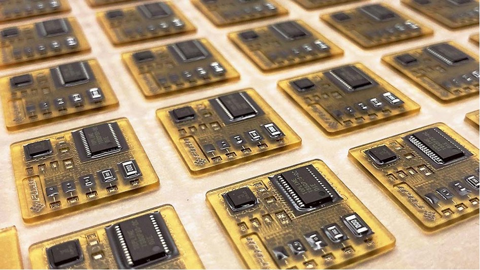
FPM-Trinity uses FUJI’s proprietary advanced process to produce high-quality electronic devices. The resin has a higher glass transition point than general ultraviolet (UV) curable resins and has a lower rate of volume expansion in high temperature environments. Formation of circuit patterns is possible by repeated printing and drying using silver nano ink that can be sintered at low temperatures. It connects layers with a structure that forms circuits along the slope of the holes. Low-temperature curable silver paste is used for conduction instead of solder. Meanwhile, the underfill is filled around the component to ensure mechanical strength.
The company is developing a fully automated process to manufacture multi-layered boards, which is currently in the process verification stage.
Partner Agreement
To promote AME, FUJI and J.A.M.E.S. GmbH of Germany signed a partner agreement in May 2023. J.A.M.E.S. aims to promote the development of AME and develop AME into a technology that everyone can use. Also, it will operate the J.A.M.E.S. community. Specifically, it is a place for real-time communication where related manufacturers and users can come together to collaborate and mutually share knowledge across company boundaries.
- Share: