ASIA ELECTRONICS INDUSTRYYOUR WINDOW TO SMART MANUFACTURING
Nascent Chiplet Gains Traction in Diverse Industries
The economic benefits derived from Moore’s Law have changed, and not for the better. This shift – especially on the manufacturing side of system-on-chip (SoC) devices, has both the defense and commercial customers in the semiconductor industry wondering what will come next.
One way to extend Moore’s Law’s cost, feature, and size benefits is with multi-chip technology, now commonly known as chiplets. These modular die devices effectively prolong Moore’s Law by replacing single silicon dies with multiple smaller dies that work together in a unified packaged device.
Integrating different physical pieces of silicon die, or chiplets, into one Lego-style device at a package level has been around for some time. However, interest in this approach was greatly accelerated when Moore’s Law began to slow down at the crucial 28nm node roughly back in 2011.
Since then, many companies and industry groups have focused on the chiplet architecture, including AMD, Intel, TSMC, and the U.S. Department of Defense (DoD). These activities have aimed to reduce time to market (TTM) and the cost by integrating pre-developed and pre-tested chiplets in a package. As with past innovations in semiconductor technology development, the initial challenge was the emergence of competing proprietary designs without any agreed-upon standards. Today, new standards have emerged. This article will examine fundamental chiplet interface technology trends in aerospace and defense (A&D) and commercial spaces and promising standards.
Chiplets and Challenges
A chiplet is a die designed to be integrated into various advanced packaging with other dies (or chiplets). They can be combined into most existing package types, such as system-in-package (SiP), 2.5D (planar or vertical), or 3D-IC.
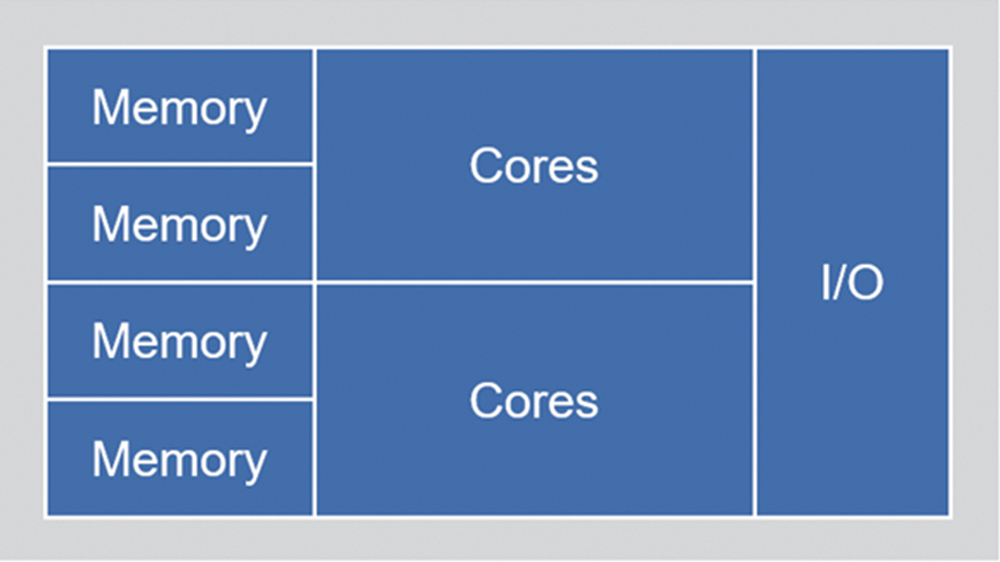
Chiplets consist of integrating separately manufactured multiple silicon components into a higher-level device, such as a SiP, that provides greater functionality and performance at a lower cost. Heterogeneous integration refers to separately manufactured parts – like chiplets – integrated into a higher-level assembly. This is opposed to the traditional monolithic chip design which is manufactured on the same die at the same time (Figure 1).
One notable advantage of the chiplet design paradigm is enabling IP reuse across different products. Flexibility is another benefit as chiplets allow different manufacturing processes for each chiplet, in contrast to traditional SoC (system-on-a-chip) designs that are restricted to a single process technology.
Today, more chipmakers are exploring the advantages of the chiplet architectures formed around existing and even advanced packaging technology. And therein lies the key, namely, how to assemble and interconnect the chiplets to meet specific requirements.
It’s not easy to use chiplets to develop multi-die designs. One major challenge is that there is no single standard die-to-die interconnect or interface approach. Instead, there are at least two competing chiplet interface technologies – Intel’s Advanced Interface Bus (AIB) and the Optical Internetworking Forum’s CEI-112G-XSR scheme.
Two other interface approaches have been proposed by the Open Domain-Specific Architecture (ODSA) industry group – Bunch of Wires (BoW) and Open High Bandwidth Interface (OpenHBI). There are also a few proprietary solutions. While each has its pluses and minuses, there is not yet a preferred standard approach to designing chiplet interfaces.
Chiplet development is also hindered by a lack of industry-wide design tool support and approved testing and assembly methods.
DoD and Chiplets
The DoD’s research arm, known as the Defense Advanced Research Projects Agency (DARPA), has long appreciated the critical connection between defensive capabilities and semiconductor technologies. For example, in 2017, DARPA initiated a chipset-based program dubbed the Common Heterogeneous Integration and IP Reuse Strategies (CHIPS).
As with similar initiatives in the semiconductor space, DARPA’s goal with CHIPS has been to drive standards and a new ecosystem in the chiplet area. Participants in the program are leading defense and chip design software and manufacturing companies.
Recently, Intel announced the completion of a multi-die chips prototype commissioned by the DoD. This prototype was built under the DoD’s State-of-the-Art Heterogeneous Integrated Packaging (SHIP) program as part of the CHIPS initiative. Under the SHIP program, Intel was tasked with developing methods for placing and connecting CPUs, FPGAs, ASICs, and government-developed chiplets, all within the same processor-type packaging. Thus, while Intel might contribute certain parts (like processors), other providers would supply the other blocks, which would come together on multiple separate dies within the same chip package.
For the SHIP program prototype, Intel used its proprietary architectures to glue together its various dies, e.g., CPU and memory cores and IO controllers. One of the future DoD’s goals under the program is to diversify its supply chain, meaning that the die interfaces will have to be more accommodating to other suppliers and less proprietary.
In general, the chiplet model offers several benefits specific to the US defense community, including the capability to acquire advanced chip architectures at relatively lower price points. While advanced chip designs are required for many defense applications, the volume of needed chips is much lower than in the commercial sector. This means that the defense community has little leverage with capacity and pricing at the semiconductor foundries. Additionally, the most advanced chips are manufactured by foundries outside the US, which presents a potential security risk.
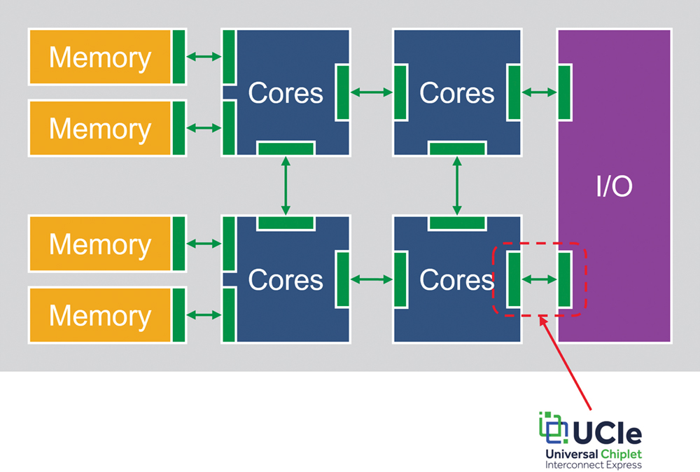
These challenges can be overcome using a chiplet development strategy (Figure 2) that allows the defense community to leverage state-of-the-art commercial technologies like FPGAs, numerous processor types, and even AI chips.
For the heterogeneous chiplet architectures to gain support in the mainstream, commercial chipmakers will need to agree on standards for die-to-die signal communications. Toward that end, several leading semiconductor vendors have come together to support an industry standard for die-to-die communications called Universal Chiplet Interconnect Express (UCIe). The spec is intended to be a common language for chiplets. In time and perhaps combined with encryption technology, the UCIe might also find applications in DOD chipsets.
Complexity at the Interconnect
Current chip interconnect trends and standards roughly fall into two categories: low-speed parallel versions for chiplets and high-speed serial versions between separate chips.
What differentiates the parallel and serial standards tends to be high-level parameters such as higher protocol layers, locations of signals on packages, and the technical voltages and slew rates. What is similar between these two signaling strategies is that both share many of the same physical signaling approaches.
Regardless of whether the challenge is a relatively low-speed, parallel signal bus between different semiconductor dies or a high-speed serial structure between two or more chips like the PCIe physical interface and related protocols, the overall system solution is complex. The physical layer components can use several different protocols to handle data communication on a network.
For the chiplet architecture to succeed, there must be standard interfaces to allow the global chipmaker ecosystem to participate. Intel has licensed its Advanced Interface Bus (AIB) technology to the UCIe program to enable heterogeneous integration of multiple die into a single package. Similarly, the CXL (compute express link) has emerged as the leading chip-to-chip protocol layer.
The AIB interconnect scheme aims to provide a high-speed and flexible way of interconnecting chips and chiplets. It’s important to note that this is a different approach from device-to-device interfaces over the last 25 years, whose aim was to use complex circuits to push high speed through a few wires, such as PCI Express. Instead, the AIB uses a very wide parallel interface supported by new high-density packaging technology. By running each wire of the interface at a relatively low speed, the circuitry for each transmitter and receiver is greatly simplified and uses minimal silicon area. There will be more discussion on this point later in the article.
Interestingly, some have argued that the UCIe physical layer (Figure 3) is superior to PCIe if bandwidth is considered over power. The first version of UCIe appears several times faster than PCIe over the same distance within a limited number of physical interfaces. UCIe has the potential to be even faster than PCIe relative to distance. The key word here is “distance,” as UCIe is designed for a very short distance on a chip’s substrate, while PCIe is implemented at the motherboard level. On the board level, data runs over a longer distance and has different electrical requirements.
Universal Chiplet Interconnect Express (UCIe)
Several years ago, a consortium of leading industry chipmakers announced the UCIe (Universal Chiplet Interconnect Express) as a new die-to-die interconnect to provide an open, multivendor chiplet ecosystem. In March 2022, the ratified UCIe 1.0 specification was released, covering the physical I/O layer, die-to-die adapter layer, and a software protocol stack that leverages the existing PCIe and CXL industry interconnect standards:
- Physical Layer: The electrical interface to the package media, including the transmitter and receiver components.
- Die-to-Die Adapter Layer: The mechanism handles link management, protocol arbitration, and negotiations.
- Protocol: This layer governs data transmissions by implementing one or more UCIe-supported protocols, including PCIe and CXL.
Both the PCIe and CXL protocols – the latter built on top of PCIe 5.0 – run on the UCIe physical interconnect. One goal of the UCIe is to accomplish at the chip package level what the PCIe interconnect has achieved for decades at the printed circuit board (PCB) level. The advantage of interconnecting systems and IP at the chip package level rather than the board level is to significantly reduce power consumption, improve bandwidth performance, and eventually lower the cost of the device.
Even though Intel donated its AIB PHY to the UCIe standard, the latter is meant to be package-technology agnostic. But this will not be an easy goal to achieve, given the wide range of different packaging technologies. For this to work, chiplets must be interoperable, meaning they can communicate and share data with one another. In addition to the UCIe standard, the compute express link (CXL) has emerged as a possible standard for the chip-to-chip protocol layer.
Other organizations have focused on the UCIe architecture. For example, the Open Compute Project (OCP) has a working group called the Chiplet Design Exchange (CDX). The charter of that group is an open ecosystem to help answer questions between vendors providing chiplet IPs into an integrated package and their ultimate delivery approach. It is the delivery models that need to be defined into a standard, such as thermal packaging models and test patterns for the packaged chiplets.

Design and Testing challenges
Designing for chiplet architectures is a more diverse engineering exercise than preparing for a single-chip SoC system. Early-stage design space explorations require simulators, especially for multi-chiplet devices, largely due to a lack of chiplet interconnect models. Existing advanced circuit design tools and circuit simulation software are needed to help development teams address signal complexity, the inherent density of chiplet structures, and heterogeneous interface technologies.
In addition to testing the parallel interfaces of the chiplet, testing of serial PCIe 4.0 and 5.0 transmitter (Tx), receiver (Rx), and channel physical layers and protocols are also needed to speed up the post-silicon validation. Advanced PCIe 6.0 input/output (I/O) signal technology will deliver even higher-performance I/O interfaces. The next-generation PCIe will also enable additional innovations, including accelerator interconnects like CXL and on-chip communications like UCIe. PCIe 6.0 capable protocol analyzer and exerciser test equipment are critical to accelerating the development, deployment, and dissemination of high-performance I/O technologies throughout the chip-making industry.
Summary
Until recently, only the largest chipmakers had the budget and interest in exploring the advantages of chiplet architectures, using in-house approaches, proprietary interconnect intellectual property (IP), and assembly techniques. However, the rise of interconnect standards such as UCIe and OCP’s Bunch-of-Wires lowers the barriers of entry for smaller firms – in both the defense and commercial markets – to contribute to the chiplet ecosystem.
About this Article
The author is Ben Miller, Product Marketing Manager for Digital Products, Keysight Technologies
–28 March 2024-
- Share: