ASIA ELECTRONICS INDUSTRYYOUR WINDOW TO SMART MANUFACTURING
Multi-Beam Mask Writer Cuts Tact Time of IC Process
Manufacturers are developing semiconductors toward the circuit line width and the gate length of 3nm. Therefore, the extreme ultraviolet (EUV) exposure equipment supporting further miniaturization is becoming necessary. Here, the exposure process involves the transfer of mask pattern to the photoresist (photosensitive material) film on the wafer.
Mainstream in IC Manufacturing
The MBMW Series multi-beam mask writer of JEOL Ltd. draws a pattern on a photomask with an electron beam in the process of applying EUV to transfer the circuit. The company expects this to become the mainstream in advanced semiconductors manufacturing, which demands shorter lead time.
In the joint development with IMS Nanofabrication GmbH of Austria, JEOL oversees the platform that will be the stage of the mask and the transport part that handles it. IMS supplies the electron gun for the beam irradiation.
The capacitor lens spreads the electron beam generated from the electron gun and divided into 262,000 beams through 512´512 apertures (holes). The aperture plate system (APS) turns the voltage On and Off when the beam passes, and controls which beam goes to the blanks.
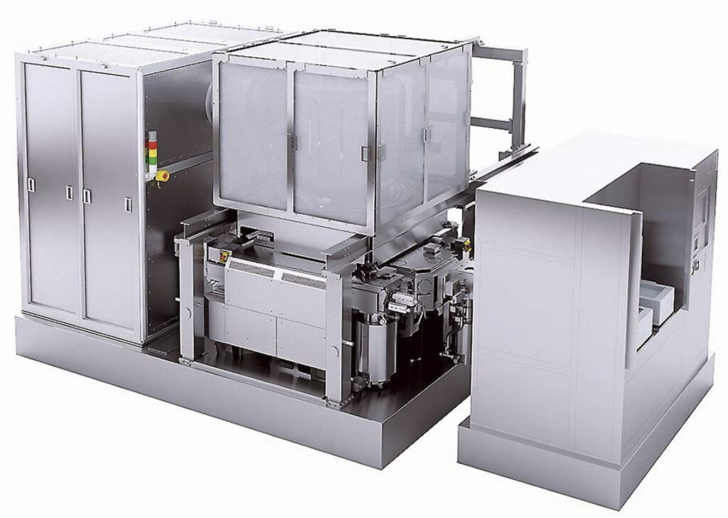
A major feature is that the acceleration voltage of the electron beam is set in two stages. The electron beam irradiated at 5keV from the beam source accelerates to 50keV after passing through the APS and irradiates the blanks. Its design avoids damage caused by the irradiation of a high voltage beam on the APS containing electronic circuits and to extend the lifetime of the APS.
The amount of exposure required supplements to the sensitivity of the resist. With the decrease in the sensitivity of the resist applied to the blanks, the accuracy of the patterning becomes higher in terms of the resolution and the edge roughness (edge deviation).
Eyes Increased Orders
Low-sensitivity resist, however, requires a large amount of exposure. At present, the mainstream variable shaped beam (VSB) drawing device has a single beam, and the exposure amount is determined by the shot time. Exposing the low-sensitivity resist requires long drawing time.
For cutting-edge masks such as EUV masks, the mask pattern is quite challenging. Therefore, when drawing with VSB, the number of shots increases significantly, inevitably making the drawing time very long.
In MBMW, the drawing time is constant regardless of the amount of exposure (resist sensitivity) and the amount of pattern data. When drawing a complicated and large-amount pattern using a low-sensitivity resist, it is possible to complete the drawing in an overwhelmingly short time in comparison with the VSB method.
Orders for the multi-beam mask writer were 14 units in 2020. JEOL expects the orders to increase to 18 units this year. In addition to the head office factory in Akishima, Tokyo, the new factory in Musashimurayama will produce MBMW from the second half of this year. Both factories aim to produce more than 20 units a year.
- Share: