ASIA ELECTRONICS INDUSTRYYOUR WINDOW TO SMART MANUFACTURING
New OMRON Inspection System Gets Innovation Honor
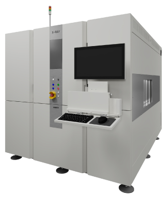
OMRON Corporation has announced that the VT-X950 automatic CT-type X-ray inspection system was awarded the Minister of Education, Culture, Sports, Science and Technology Award at the 53rd Japan Industrial Technology Awards, sponsored by Nikkan Kogyo Shimbun. Specifically, the VT-X950 automatic CT-type X-ray inspection system inspection technology for semiconductor chiplets was released in Nov. 2023.

High-Speed, High-Precision Inspection
By combining OMRON’s proprietary control and image processing technologies, VT-X950 enables high-speed, high-precision inspection of advanced semiconductor packages. Also, OMRON combined the continuous imaging technology*1 and the high sensitivity camera by seamless control of the control equipment constituting the device. Accordingly, the generated 3D image features high resolution and is easy to distinguish. With the high resolution of imaging at 0.2μm, it is possible to visualize the solder quality of μBump*2 and C4Bump*3 used in the 3D mounting of each semiconductor package. In addition, the high-speed generation of modeling utilizing the most advanced 3D inspection technology used in medical CT scanning enables in-line quality inspection, which was difficult at the manufacturing site.
By utilizing OMRON’s proprietary AI technology, automatic optimization of the setting of imaging conditions for inspection was possible. Also, it enabled the automation of inspection program creation, which was difficult until now for experienced technicians.
The comments of the judging panel of the Japan Industrial Technology Award are as follows:
“It is a technology necessary for the advancement of the semiconductor industry. Also, it is an important automated inspection technology for the improvement of semiconductor performance.”
“It is possible to perform in-line inspection at 100 times higher speed than a typical analyzer.”
“The minimum resolution per pixel for CT type X-ray inspection was improved from 0.3μm to 0.2μm”
Further advances in semiconductor miniaturization and performance are expected. Thus, advanced inspection technology is essential for stable production and high quality. In addition to improving productivity at manufacturing sites, OMRON enriches the future for people, industries, and the world through innovative automation.
*1: Technology for imaging stereoscopic images without stopping while moving
*2: Bump electrode formed at a narrow pitch for bonding IC devices together
*3: Controlled Collapsed Chip Connection (C4) A bump-shaped conductor protrusion is formed on the substrate electrode and bonded to the wafer
-17 April 2024-
- Share: