ASIA ELECTRONICS INDUSTRYYOUR WINDOW TO SMART MANUFACTURING
Samsung Blazes Trail to in-Memory Neuromorphic ICs
Reverse-engineering human brains is to mimic the structure and function of neural network in the brain on a silicon wafer to create a so-called neuromorphic AI chips.
Although it is still a long distant future, Samsung Electronics has laid the ground work for it, authoring a thesis titled as “Neuromorphic Electronics Based on Copying and Pasting the Brain”.
In the thesis printed on Nature Electronics, Samsung suggests an innovative way to use a nano-electrode array to copy the brain’s neuronal connection map and then paste it on a memory chip using a 3D stacking and deposition technology as well as a 3D TSV packaging technology.
The thesis is co-authored by a group of well-known academics and seasoned engineers, including Donhee Ham, fellow of Samsung Advanced Institute of Technology (SAIT) and professor of Harvard University, Hongkun Park, professor of Harvard University, Sungwoo Hwang, president and CEO of Samsung SDS and former Head of SAIT, and Kinam Kim, vice chairman and CEO of Samsung Electronics.
The theory is straightforward. The human brain is made up of a large number of neurons, and each neuron is wired together to create a wiring map, a sort of control tower to supervise the brain’s functions like cognition, facile learning, and adaptation.
At issue is how to copy, or mimic the wiring map and then memorize it in a non-volatile memory chip. To work out this challenge, Samsung has been working together with Harvard University since 2019 and Dr, Ham of Samsung and Dr, Park of Harvard University has jointly developed what’s called as a nano-electrode array, which can be implanted onto human brain neurons. The microscopic array is so sensitive that it can read and record ultra-minute electrical signals occurring at connecting points of each neuron. This reading can help extract and copy the brain’s wiring map.
Neuronal Connection Map
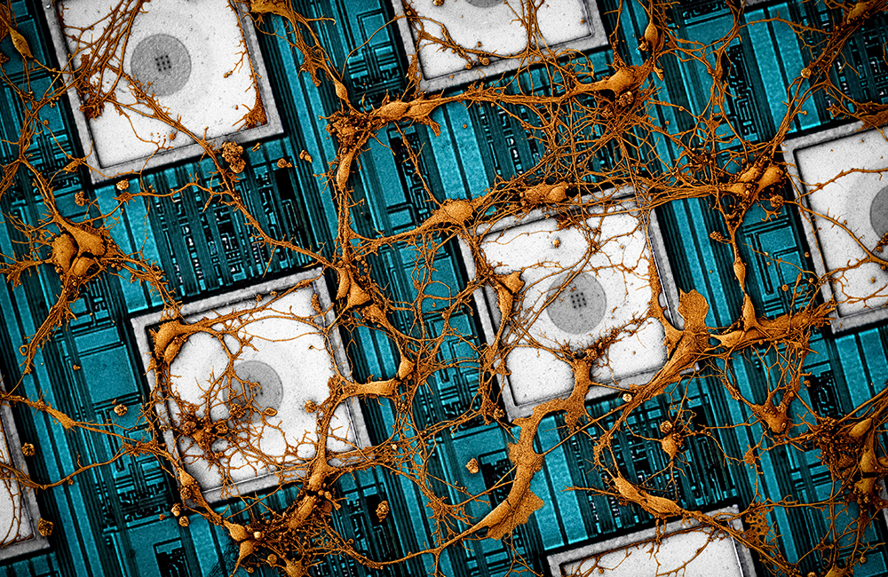
The second challenge is how to paste the map onto such non-volatile memory chips like NAND flash-based SSD or resistive random access memory, or R-RAM.
Samsung believes that it can be done by programming each memory so that its conductance represents the strength of each neural connection in the copied map. Then, the network of specially-engineered non-volatile memories can learn and express the neuronal connections map. This is a scheme that directly downloads the brain’s neuronal connection map onto the memory chip.
As the human brain has an estimated 100 billion or so neurons, and a thousand or so times more synaptic connections, however, the ultimate neuromorphic chip will require 100 trillion or so memory cells.
Integrating such vast number of memories on a single chip would be made possible by 3D integration of memories, the technology led by Samsung that opened up a new era for memory industry.
Leveraging its leading experience in chip manufacturing, Samsung is planning to continue its research into neuromorphic engineering, in order to extend Samsung’s leadership in the field of next generation AI semiconductors.
“The vision we present is highly ambitious,” said Dr. Ham. “But working toward such a heroic goal will push the boundaries of machine intelligence, neuroscience, and semiconductor technology”
- Share: