ASIA ELECTRONICS INDUSTRYYOUR WINDOW TO SMART MANUFACTURING
Synopsys to Boost Innovative IC Grit on TSMC Process
Synopsys, Inc. has announced broad EDA and IP collaborations with TSMC for advanced node designs. Consequently, they have been deployed across a range of AI, high-performance computing, and mobile designs.
Among the newest collaborations is a co-optimized Photonic IC flow, addressing the application of silicon photonics technology in the quest for better power, performance, and transistor density.
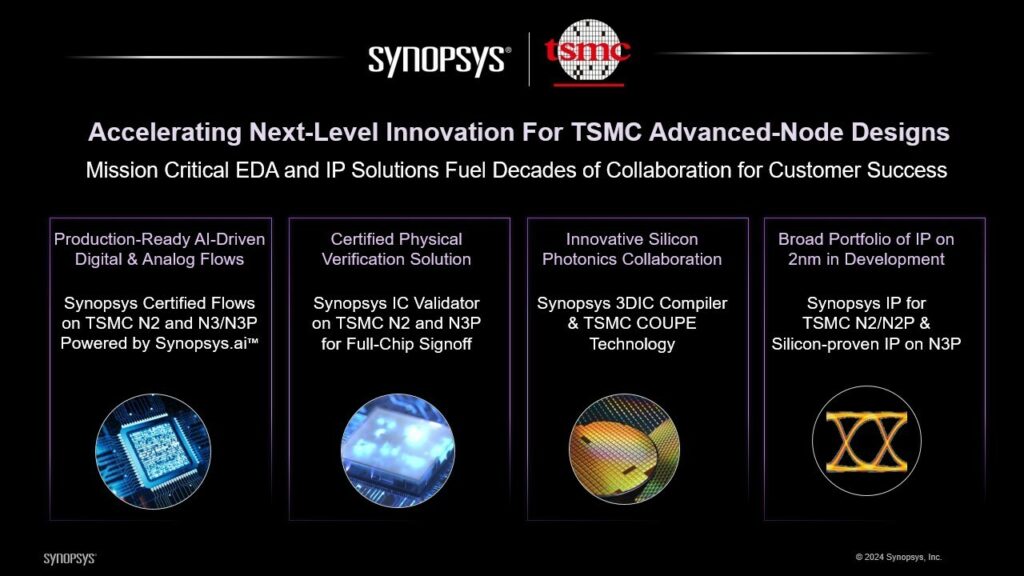
In addition, Synopsys also noted the industry’s confidence in its digital and analog design flows, production-ready for TSMC N3/N3P and N2 process technologies. The two companies are collaborating on next-generation AI-driven flows, including Synopsys DSO.ai™, for design productivity and optimization. In addition, Synopsys is developing a broad portfolio of Foundation and Interface IP on TSMC N2/N2P. In a related announcement today, Keysight, Synopsys, and Ansys introduced a new integrated radio frequency (RF) design migration flow from TSMC’s N16 process to its N6RF+ technology.
Next-Level Innovation in Chip Designs
“The advancements in Synopsys’ production-ready EDA flows and photonics integration with our 3DIC Compiler, which supports the 3Dblox standard. Combined with a broad IP portfolio enable Synopsys and TSMC to help designers achieve the next level of innovation for their chip designs on TSMC’s advanced processes,” said Sanjay Bali, vice president of strategy and product management for the EDA Group at Synopsys.
“The deep trust we’ve built over decades of collaboration with TSMC has provided the industry with mission-critical EDA and IP solutions. (Thus) deliver(ing) compelling quality-of-results and productivity gains with faster migration from node to node.”
Meanwhile, Dan Kochpatcharin, head of Design Infrastructure Management Division at TSMC said the close collaboration with Open Innovation Platform (OIP)® ecosystem partners enables customers address the most challenging design requirements. This, Kochpatcharin said, made possible with at the leading edge of innovation from angstrom-scale devices to complex multi-die systems across a range of high-performance computing designs. “Together, TSMC and Synopsys will help engineering teams create the next generation of differentiated designs on TSMC’s most advanced process nodes with faster time to results.”
Certified Digital, Analog Flows on Advanced Nodes
Synopsys has production-ready digital and analog design flows for TSMC N3P and N2 process technologies. In fact, they have been deployed across a range of AI, high-performance computing, and mobile designs.
The AI-driven analog design migration flow enables rapid migration from one process node to another. A new flow is available for TSMC N5 to N3E migration, adding to Synopsys’ established flows for TSMC N4P to N3E and N3E to N2 processes.
In addition, interoperable process design kits (iPDKs) and Synopsys IC Validator™ physical verification runsets are available. Thus, enabling design teams to efficiently transition designs to TSMC advanced process technologies.
Moreover, Synopsys IC Validator enables full-chip physical signoff to handle the increasing complexity of physical verification rules. Synopsys IC Validator is now certified on TSMC N2 and N3P process technologies.
Faster Data Transmission for Multi-Die Designs with Photonic ICs
The high volume of data processing for AI training requires low-latency, power-efficient, and high-bandwidth interconnects. In other words, driving the adoption of optical transceivers and near-/co-packaged optics using silicon photonics technology. Synopsys and TSMC are developing end-to-end multi-die electronic and photonic flow solutions for TSMC’s Compact Universal Photonic Engine (COUPE) technology to enhance system performance and function. This flow spans photonic IC design with Synopsys OptoCompiler™ and integration with electrical ICs utilizing Synopsys 3DIC Compiler and Ansys multiphysics analysis technologies.
Speed Time-to-Market with Broad IP Portfolio N2 and N2P
Meanwhile, Synopsys is developing a broad portfolio of Foundation and Interface IP for the TSMC N2 and N2P process technologies. This will enable faster silicon success for complex AI, high-performance computing, and mobile SoCs.
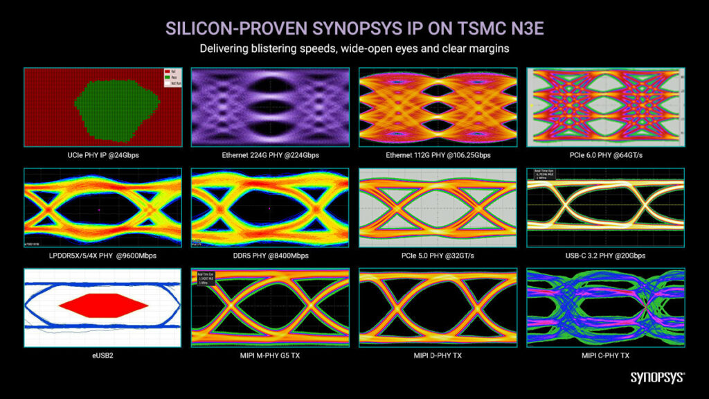
Furthermore, tere are available high-quality PHY IP on N2 and N2P, including UCIe, HBM4/3e, 3DIO, PCIe 7.x/6.x, MIPI C/D-PHY and M-PHY, USB, DDR5 MR-DIMM, and LPDDR6/5x. These allow designers to benefit from the PPA improvements of TSMC’s most advanced process nodes.
In addition, Synopsys provides a silicon-proven Foundation and Interface IP portfolio for TSMC N3P, including 224G Ethernet, UCIe, MIPI C/D-PHY and M-PHY, USB/DisplayPort and eUSB2, LPDDR5x, DDR5, and PCIe 6.x, with DDR5 MR-DIMM in development.
Synopsys IP for advanced TSMC processes has been adopted by dozens of leading companies to accelerate their development time.
–26 April 2024-
- Share: