ASIA ELECTRONICS INDUSTRYYOUR WINDOW TO SMART MANUFACTURING
FUJIFILM Props up Nanoimprint Lithography with New Resist
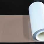
FUJIFILM Corporation has launched the Nanoimprint Resist, a semiconductor material compatible with nanoimprint lithography semiconductor manufacturing technology. FUJIFILM Electronics Materials Corporation, a core company in the electronic materials business, will offer the new film in Japan.
There is a growing demand for advanced semiconductors with higher performance. Primarily, it is driven by high-speed, high-capacity communications through 5G/6G. Also, the expansion of autonomous driving and the spread of AI and metaverse are contributing factors. Nanoimprint lithography was introduced last year as a new manufacturing technology that can produce high-performance semiconductors at low cost and with low power consumption. Unlike photolithography, nanoimprint lithography does not require development and rinse processes or complex optical systems for exposure. Nanoimprint lithography is seen to expand particularly in the advanced semiconductor segment. Its ability to produce high-performance semiconductors at lower cost and with lower power consumption than photolithography will drive this.

Structure and Features
Mainly, the new Nanoimprint Resist features a molecular structure optimal for nanoimprint lithography. It was developed through the analysis of the resist’s flow behavior during the imprinting process and the interaction of resist with wafer surfaces and masks. To achieve this, the company utilized the knowledge and technology cultivated in the development of photoresists. Also, the Nanoimprint Resist can quickly and uniformly fill the complex circuit patterns engraved on the mask. It can also transfer and form nanometer-scale circuit patterns in a short time.
Furthermore, after curing by UV radiation, the Nanoimprint Resist shows excellent mold-releasing properties that do not cause loss of circuits even when the mask is removed at high speed. This enables the improvement of throughput – patterning throughput per hour – and yield improvement due to low defects. Mainly, these issues hinder the practical application of nanoimprint lithography. Also, Nanoimprint Resist contributes to cost reduction and energy saving in the manufacturing of advanced semiconductors.
In addition, Fujifilm utilized the technology cultivated through the development of industrial inkjet printers. Accordingly, it has realized a formulation design that allows the optimum amount of droplets to be applied to the wafer surface using an inkjet method. Compared to the spin-coating method*1 used in the current manufacturing process, the amount of resist used can be reduced to approximately 1/100*2. Also, the Nanoimprint Resist uses a hydrocarbon compound as a release agent instead of per- and polyfluoroalkyl substances (PFAS). Specifically, PFAS is a group of synthetic chemicals. Their use is increasingly regulated due to concerns over their impact on the environment and ecosystems.
By providing its Nanoimprint Resist, Fujifilm will continue to promote the spread and expansion of new manufacturing technology that contributes to cost reduction and power saving in leading-edge semiconductor manufacturing.
Mainly, Fujifilm provides photoresists, process chemicals, polyimides, and other process materials for semiconductor manufacturing from front-end to back-end processes. It also offers Wave Control Mosaic (WCM) such as color filter materials for image sensors. It is a semiconductor materials manufacturer providing one-stop solutions covering from leading-edge to legacy semiconductors. Thus, the company is working to meet the needs of customers and solve their issues. With the addition of the Nanoimprint Resist suitable for cutting-edge semiconductors to its product lineup, Fujifilm will continue to contribute to the further development of the semiconductor industry. To this end, it will offer these wide-ranging products and develop products compatible with new manufacturing technologies.
*1 A method of creating a resist thin film by dropping resist onto a wafer and rotating the wafer at high speed.
*2 Trial calculation by Fujifilm
-07 May 2024-
- Share: