ASIA ELECTRONICS INDUSTRYYOUR WINDOW TO SMART MANUFACTURING
Canon Launches Revolutionary Chip Manufacturing System
Canon announced the launch of the FPA-1200NZ2C nanoimprint semiconductor manufacturing equipment, which executes circuit pattern transfer. This is considered the most important semiconductor manufacturing process.
Over the years, Canon has released several photolithography systems. This time, it has brought to market the semiconductor manufacturing equipment with nanoimprint lithography (NIL) technology. With these offerings, Canon expands its lineup of semiconductor manufacturing equipment. Accordingly, it meets the needs of a wide range of users by handling a broad array of equipment from the most advanced semiconductor devices to the existing devices.
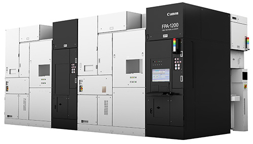
Conventional photolithography equipment transfers a circuit pattern by projecting it onto the resist-coated wafer. Meanwhile, the new product does it by pressing a mask imprinted with the circuit pattern on the resist on the wafer like a stamp. Because its circuit pattern transfer process does not go through an optical mechanism, fine circuit patterns on the mask can be faithfully reproduced on the wafer. Thus, it forms complex two- or three-dimensional circuit patterns in a single imprint1, which reduces the cost of ownership (CoO).
Canon’s NIL technology enables patterning with a minimum linewidth of 14nm2. Specifically, this is equivalent to the 5-nm-node3 required to produce the most advanced logic semiconductors currently available. Furthermore, with further improvement of mask technology, NIL will enable circuit patterning with a minimum linewidth of 10nm, which corresponds to 2-nm-node.

Moreover, the new product employs a newly developed environment control technology. Mainly, this technology suppresses the contamination with fine particles in the equipment. This enables high-precision alignment, which is necessary for the manufacture of semiconductors with an increasing number of layers, and reduction of defects due to fine particles. Also, it enables the formation of fine and complex circuits, contributing to the manufacture of cutting-edge semiconductor devices.
Additionally, the new product does not require a light source with a special wavelength for fine circuit. Thus, it can significantly reduce power consumption compared to photolithography equipment for currently available advanced logic semiconductors (5-nm-node with 15 nm linewidth), thereby contributing to CO2 reduction.
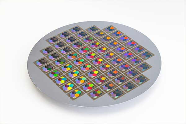
Also, it suits a wide range of applications. Among them are metalenses4 for XRs with microstructures of tens of nanometers, in addition to logic and other semiconductor devices.
1 A pattern-forming process of nanoimprinting.
2 one billionth of a meter.
3 nm-node: a generation of semiconductor technology
4 An element with the same function as a lens by controlling light with a fine structure smaller than the wavelength of visible light.
- Share: