ASIA ELECTRONICS INDUSTRYYOUR WINDOW TO SMART MANUFACTURING
DISCO Yields Large Diamond Wafer with New Process
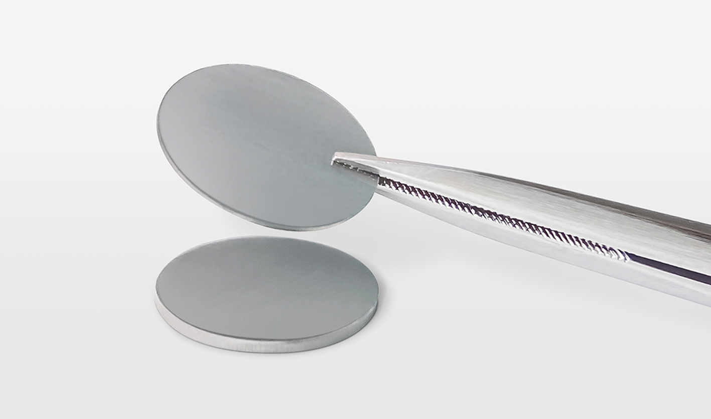
DISCO Corporation, a Japanese semiconductor manufacturing equipment manufacturer, has announced the development of a new process for diamond wafer manufacturing. Specifically, the KABRA process is an ingot slicing method that uses laser technology. Mainly, this process contributes to increasing the diameter of diamond wafers.
Developmental Background
Diamond is often called the “ultimate semiconductor material” due to its superior material characteristics compared to silicon (Si), silicon carbide (SiC), and gallium nitride (GaN). Particularly, as diamond has excellent insulation strength and heat conductivity, it is considered a good material for power semiconductors. Device development is underway at various research institutes.
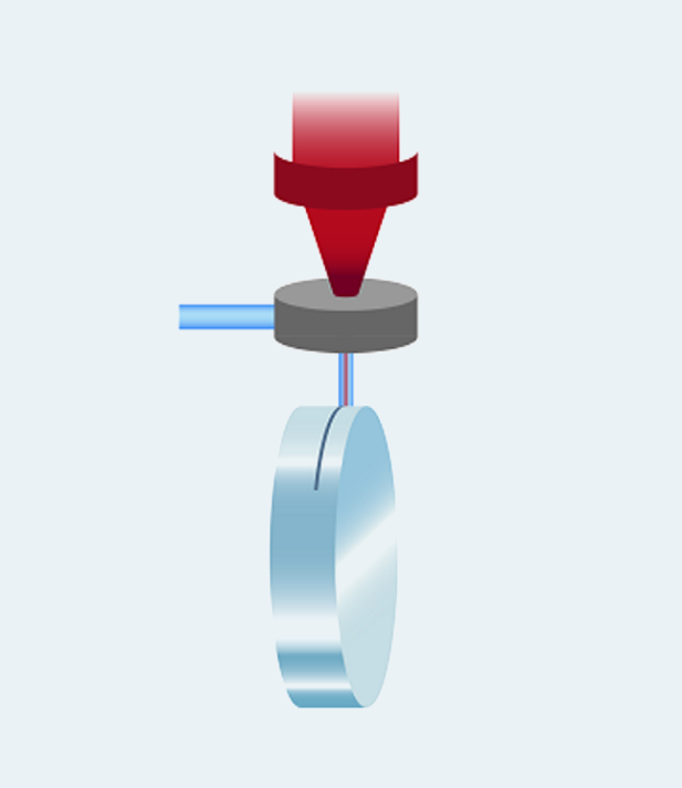
On the other hand, as it is an extraordinarily hard material, its difficulty to process mechanically has been common knowledge. Therefore, laser became the general method used to slice wafers from a diamond crystalline ingot. However, in conventional laser slicing method, the ingot is processed from the sidewall. Thus, the ingot diameter poses some limitations, and increasing it, was a challenge. With KABRA slicing by DISCO, there is no limitation on the ingot diameter. This is so as the laser is irradiated from the upper surface of the ingot, making it possible to increase the ingot diameter.
Features
Supports large-diameter ingots exceeding Φ50 mm
With the conventional method where the laser is irradiated from the sidewall of an ingot (Figure 1), the largest supported diameter was approximately Φ30 mm. However, with the KABRA method (Figure 2), as the laser is irradiated from the upper surface of the ingot, there is no limitation on the ingot diameter.

Splitting wafers with a thickness of 100µm or less is possible
By irradiating the laser at a shallow depth from the upper surface of the ingot, it is possible to split thin wafers. Therefore, a larger number of split wafers can be expected compared to the conventional method.
Achieves equivalent or higher throughput compared to the conventional method
Moreover, the splitting speed is equal to or faster than the conventional method, achieving lower processing costs. In addition, 45 patents related to this technology have been registered.
Today, test cuts are already available.
-22 May 2024-
- Share: