ASIA ELECTRONICS INDUSTRYYOUR WINDOW TO SMART MANUFACTURING
SiC, GaN Lead Race in Wide-Gap Semiconductor Power Devices
In recent years, the development of wide-gap semiconductor power devices has become active. SiC- MOSFETs and lateral GaN-HEMTs, which surpass the performance of Si power devices, have already been put to practical use. The characteristics and applications of those devices, as well as the current status and issues of vertical GaN devices, Ga2O3 and diamond devices aiming for higher performance are presented.
Introduction
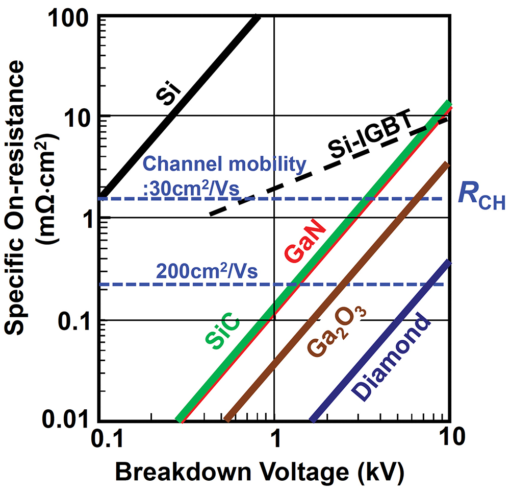
With the electrification associated with decarbonization and the expansion of electric energy consumption in recent years, power electronics, which control electric energy, is attracting attention. Especially, higher efficiency of power devices is required, which are key devices that constitute power electronics. Si power devices have been conventionally used, and their performance is still improving today. But the limits of materials are becoming apparent for groundbreaking performance improvements. Therefore, wide-gap semiconductor power devices, such as SiC and GaN, are attracting attention. The breakdown electric field strength of these wide-gap semiconductors is more than 10 times that of Si, and when compared with the same breakdown voltage, the thickness of the drift layer required to hold the voltage is less than 1/10, and the on-resistance of the device can be reduced. Fig. 1 shows the theoretical limits of the specific on-resistance for the breakdown voltage of the drift layer. Compared to MOSFETs of Si, which are unipolar devices, the on resistance of SiC and GaN is theoretically 1/1000. Furthermore, Ga2O3 and diamond can be expected to have even lower on-resistance. Therefore, if a wide-gap semiconductor power device can be made, there is a possibility of realizing a power device with an epoch-making low on-resistance (that is, high efficiency). However, to make it a power device, it is necessary to develop various issues. This paper summarizes the current status, issues and applications of wide-gap semiconductor power devices of SiC, GaN, Ga2O3 and diamond, which are under development.
SiC Power Devices
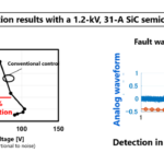
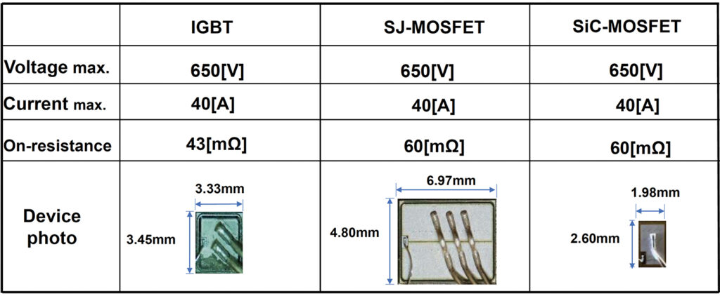
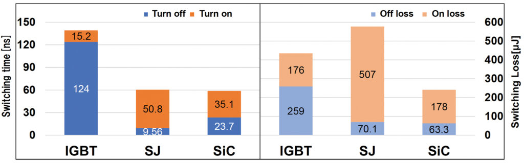
Among these wide-gap semiconductors, SiC is the most advanced in device development[1]. Therefore, the switching characteristics of commercially available power devices will be evaluated and the characteristics of SiC-MOSFETs will be clarified. As Si power devices, IGBTs and super junction MOSFETs, which have the same breakdown voltage of 650V and current capacity of 40A as SiC-MOSFETs, were selected, and their switching characteristics were compared in a double pulse test. Table 1 shows the specifications and chip photos of the selected devices. On-resistance is the lowest for Si-IGBT, which is a bipolar transistor, and is the same for SJ-MOSFET and SiC-MOSFET. The biggest difference between the three devices is the chip size. When converted to current density, they are 348A/cm2 (IGBT), 120A/cm2 (SJ), and 777A/cm2 (SiC), indicating that SiC has the highest current density. It is thought that the low on-resistance performance shown in Fig. 1 of SiC was allocated to chip size reduction and cost reduction. In addition, a small chip size leads to a reduction in input capacitance, contributing to an improvement in switching speed. Figure 2 shows the results of the double pulse test. Since the IGBT is bipolar, the turn-off time is long due to tailing of the current, so the turn-off loss is also the largest. On the other hand, the SJ-MOSFET has a long turn-on time due to severe ringing at turn-on, resulting in a large turn-on loss. SiC-MOSFET shows good values for both switching speed and switching loss, showing the highest performance. In addition, devices with 1200V rating also show excellent characteristics, and the adoption of SiC-MOSFETs will likely expand in the future. Future issues for the SiC power device are as follows: 1) further reduction in on-resistance by improving channel mobility; 2) increase in current capacity per chip; 3) improvement in substrate quality and larger diameter; and 4) cost reduction.
GaN Power Devices
GaN power devices have lateral and vertical structures, and the lateral structure is being put to practical use[2, 3]. On the other hand, the vertical structure is expected to have high performance, but it is still in the development stage and process technology is being developed. Present conditions of both type devices are presented followings.
Lateral GaN power devices
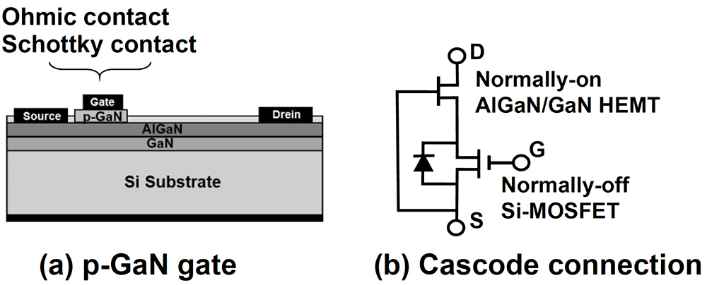
The lateral structure is a structure in which current flows along the surface, and devices rated at 650V, which cannot be achieved with Si, are also available on the market. This is because the lateral structure device has an AlGaN/GaN heterostructure channel, which can form a very low resistance channel. In this device, a p-GaN gate structure is adopted as the gate structure to achieve normally off operation. The structure is shown in Fig. 3. There are two types of gate contacts: ohmic contact and Schottky contact (Fig.3 (a)). Due to these structural differences, different gate drive circuits are employed. The p-GaN gate structure has a feature that the temperature dependence of the threshold voltage is extremely low, but it has a weakness that the threshold voltage is 1 to 2V and cannot take high value over 3V. On the other hand, an another normally-off device is also available. This structure is that the low-voltage Si-MOSFET and the normally-on AlGaN/GaN lateral device are connected as shown in Fig. 3 (b) (this connection is called cascode connection) and it can be treated as a normally-off three-terminal device. This structure has the advantage of using a normal MOSFET drive circuit for the gate drive circuit, and since the threshold voltage is determined by the Si-MOSFET, it is possible to have a threshold voltage of 3V or higher. However, since the Si-MOSFET is in series with the circuit, it also has the drawback of increasing the on-resistance. The greatest feature of these lateral structure devices is the capability of high-speed switching. Therefore, the size of the power supply can be reduced, and it is recently used in chargers for PCs and mobile phones. Lateral structure devices are suitable for power applications up to about 10kW, and have many applications including consumer products. GaN lateral power devices are fabricated by hetero-growth on a Si substrate via a buffer layer. Therefore, there is an advantage of cost reduction by increasing the diameter. Sapphire substrates are also used for low power applications. The lateral structure is also suitable for device integration, and the development of higher functionality through integration will be the direction of development in the future.
GaN vertical power devices
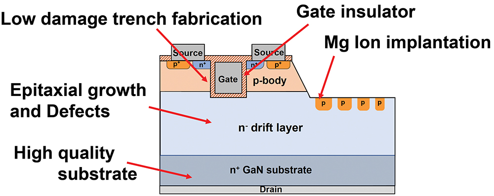
Vertical GaN power devices are characterized by low on-resistance under high breakdown voltage similar to SiC-MOSFET. The on-resistance performance of the drift layer calculated from the physical properties is almost the same as that of SiC, as shown in Fig. 1. However, the on-resistance of a power device is determined not only by the resistance of the drift layer, but also the contribution of the channel resistance of the gate cannot be ignored. The line labeled channel mobility in Fig. 1 indicates the channel resistance determined by channel mobility. So. the on-resistance is limited by the channel mobility. In SiC-MOSFET, the channel mobility is around 30cm2/Vs, and the on-resistance is determined by the channel resistance below about 3kV. On the other hand, GaN has so far achieved higher channel mobility of about 200cm2/Vs for the MOS channel and more than 1000cm2/Vs for the HEMT channel. Therefore, GaN has the potential for even lower on-resistance than SiC. This is the motivation for developing vertical GaN power devices. However, at present, it is still in the development stage, and the elemental technologies as shown in Fig. 4 is being developed. In recent years, those elemental technologies have also been solidified, and the development of vertical GaN has shifted to device prototyping and performance verification.
Ga2O3 and diamond power device
Ga2O3 is wideband gap semiconductor that has been attracting attention in recent years.
The potential for power device is large as shown in Fig.1. Ga2O3 crystal has α-type and β-type crystal structure, and α-Ga2O3, β-Ga2O3 are used for power devices. The β-Ga2O3 is the most stable structure. N-type doping and carrier concentration control are possible, however, p-type doping was very difficult, which is a large problem. The merit of Ga2O3 is that high-quality single crystal wafers are available. Many types of devices have been tried using Ga2O3 [4-7]. However, the performances are not yet excess SiC and GaN devices. Therefore, the development phase of Ga2O3 devices is research of elemental technologies for power devices. Ga2O3 still faces many challenges in demonstrating high-performance power devices. Material properties have high potential but the future strongly depends on overcoming two major challenges. The first is a countermeasure against the lack of p-type. The second is the selection of the optimum gate dielectric.
Diamond has the highest thermal conductivity among all substances, and its critical electric field strength is about seven times higher than that of SiC and GaN. Various methods have been developed for the production of diamond substrates since artificial diamond was synthesized by the high-temperature and high-pressure method, but currently microwave plasma CVD (MPCVD) is the mainstream. The n-type and p-type doping are also realized by the MPCVD method, and P (phosphorus) and B (boron) were used for the n-type and p-type dopants, respectively. However, the carrier concentration at room temperature is low because of high activation energies of P and B which are 0.57eV and 0.37eV, respectively. B-doped p-type is widely used for device fabrication because it is easy to grow. The hole mobility of B-doped diamond has been reported to be over 1000cm2/Vs. SBDs have been fabricated using this epitaxial layer, but they are expected to be used in high-temperature environments because of the high activation energy of B[8]. In addition, in order to solve this problem in MOSFET and MESFET, the development of devices using two-dimensional hole gas (2DHG) generated on the surface of hydrogen-terminated diamond as a channel is being actively developed[9,10]. Inversion layer channel MOSFETs have also been developed using hydrogen terminations for source and drain[11]. In recent years, there have been many reports on the development of these devices, but their performance does not match the performance of conventional power devices, and the realization of practical devices still takes a lot of time.
Conclusion
Si will still maintain the main position of power devices to the near future, but, the wide gap semiconductor devices have the potential for realizing different world from Si power devices; for example, ultra-low loss power transmission electric motor airplane flying electric car high efficiency renewable energy system, etc. Each material has its own challenges, but the development of wide-gap semiconductor power devices will progress steadily, just as it did with Si.
References:
[1] T. Kimoto and H. Watanabe, Applied Physics Express 13, 120101 (2020).
[2] T. Kachi, Japanese Journal of Applied Physics 53, 100210 (2014).
[3] R. Chu, Appl. Phys. Lett., 116, 090502 (2020).
[4] M. Oka, R. Tokuda, h. Kambara, T. Tanikawa, T. Sasaki, and T. Hirita, Appl. Phys. Express, 9, 021101 (2016).
[5] M. Higashiwaki, K. Sasaki, A. Kuramata, T. Masui, and S. Yamakoshi, Appl. Phys. Lett., 100, 013504 (2012).
[6] M. H. Wong, K. Goto, H. Murakami, Y. Kumagai, and M. Higashiwaku, IEEE Electron Device Lett., 40, 431(2019).
[7] Z.Hu, K. Nomoto, W. Li, N. Tanen, K. Sasaki, A. Kuramata, T. Nakamura, D. Jena, and H. G. Xing, IEEE Electron Device Lett., 39, 869 (2018).
[8] H. Umezawa, K. Kato, S. Shikata, Appl. Phys. Express, 6, 011302 (2013).
[9] H. Kawarada, H. Tsuboi, T. Naruo, T. Yamada, D. Xu, A. Daicho, T. Saito, and A. Hiraiwa, Appl. Phys. Lett., 105, 013510 (2014).
[10] H. Umezawa, T. Matsumoto, S. Shikata, IEEE Electron Devoce, Lett., 35, 1112 (2014).
[11] T. Matsumoto, H. Kato, K. Oyama, T. Makino, M. Ogura, D. Takeuchi, T. Inokuma, N. Tokuda, and S. Yamasaki, Sci. Rep. 6, 31585 (2016).
About this Article:
The author is Tetsu Kachi of the Institute of Materials and Systems for Sustainability, Nagoya University, Nagoya, 464-8601, Japan.
- Share: