ASIA ELECTRONICS INDUSTRYYOUR WINDOW TO SMART MANUFACTURING
ADEKA Boosts Plant to Better Serve IC Demand Growth
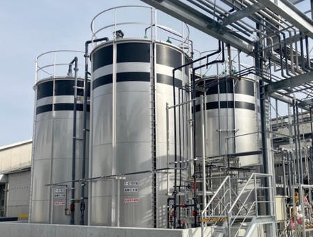
ADEKA Corporation said it has already concluded capacity expansion of its plant in Fuji City in Japan’s Shizuoka. The facility produces high-purity hydrogen peroxide for semiconductors. Accordingly, the new expanded facility will commence operation in July.
Semiconductors are essential to realize an advanced ICT society. Specifically, semiconductors play a role in AI and data centers. Demand for semiconductors is likely to improve in the future and active capital investment is propelling worldwide.
In Japan, global semiconductor manufacturers are building the momentum. Thus, manufacturing bases have been rising one after another to ensure a stable supply of materials necessary for domestic manufacturing is an issue.
Strength in Materials for ICs
ADEKA’s strength lies in advanced materials essential for semiconductor technological innovation. For that reason, it is strengthening capital investment both domestically and overseas.
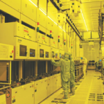
At its Fuji Plant, ADEKA manufactures hydrogen peroxide and its derivatives for electronics-related products. Among them are necessities, toiletries, and electronic devices. For semiconductors, the company manufactures high-purity hydrogen peroxide used for cleaning during manufacturing. Thus, the strengths are high-purity technology and thorough quality control compatible with semiconductor manufacturing.
“Seeing the booming domestic semiconductor business as an opportunity, we have increased our production capacity for high-purity hydrogen peroxide, for which demand is expected to increase,” said ADEKA in a statement. For that reason, the company will expect an increase in its production capacity by 1.3 times compared to before.
The ADEKA Group will contribute to the realization of an advanced ICT society not only by providing cutting-edge materials in major semiconductor manufacturing areas such as South Korea, Taiwan, and the United States. Moreover, it will provide a stable supply of products necessary for semiconductor manufacturing in Japan.
Expands Clout in Semiconductor Manufacturing
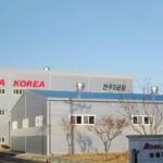
Recently, ADEKA KOREA CORPORATION, a consolidated subsidiary of ADEKA, has recently completed its expansion in Korea.
Located in Hwaseong City in Korea’s Gyeonggi Province, ADEKA has acquired the facility with a total floor area seven times larger than the previous one. In addition, the clean room, which is twice the size of the previous one, has expanded the number of ALD deposition and evaluation equipment. Moreover, it will function as a specialty for evaluation and analysis of cutting-edge semiconductor deposition materials.
“We plan to double our equipment and personnel by 2030,” said ADEKA in a statement.
The ADEKA Group’s research and development of new semiconductor materials will continue at Japan’s Oku Central Research Institute in Arakawa-ku, Tokyo.
In early 2026, ADEKA plans to construct and relocate a new research building within the Kuki Area Development Research Institute in Kuki City, Saitama Prefecture. Specifically, this will expand its share of materials for the front-end processes of the group’s main products, semiconductor memory, and logic semiconductors. “We aim to expand our field to include post-process materials,” said ADEKA.
27 May 2024
- Share: