ASIA ELECTRONICS INDUSTRYYOUR WINDOW TO SMART MANUFACTURING
Hitachi High-Tech Eyes Large Specimens with New FE-SEM
Hitachi High-Tech Corporation has launched the SU3900SE and SU3800SE High-Resolution Schottky Scanning Electron Microscopes, which provide highly accurate and efficient observation of large and heavy specimens at the nano level.
The SU3900SE specimen stage was redesigned to enable operators to observe heavy specimens up to 5kg. The specimen stage is the largest in Hitachi High-Tech’s scanning electron microscope (SEM) offerings, making it suitable for large specimens up to 300mm in diameter and 130mm in height. This is around 1.5 times larger than its SU5000 predecessor. Further, this reduces the need for additional specimen preparations such as cutting specimens, helping to make the overall process more efficient. In addition to enabling the observation of large and heavy specimens, the specimen is controlled by a 5-axis motorized stage (X, Y, Z, tilt, and rotation).
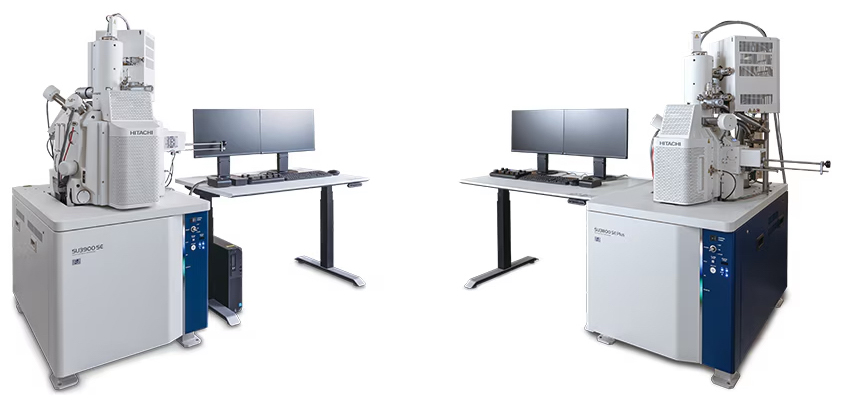
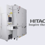
SU3900SE (left) and SU3800SE (right)
Also, these new instruments feature a camera navigation function that stitches together separate images to allow viewing of the entire specimen. Thus, it helps operators with identifying points of interest when observing large specimens, providing improved usability.
As part of Hitachi High-Tech’s commitment to working towards a sustainable society, the environmentally friendly design reduces CO2 emissions by reducing power consumption to 2kVA, around 50% compared to existing FE-SEM models, while still maintaining high-performance requirements.
Product Development Background
Mainly, SEMs are instruments for observing microstructures on the surface of materials. They are widely used in research and development, manufacturing, and quality control in a variety of fields, including nanotechnology and biotechnology. In particular, there is a growing need for high-resolution Schottky field emission scanning microscopes (FE-SEMs) with a broader range of capabilities than what is currently available.
When observing large and heavy specimens, such as iron, steel, and other industrial materials or vehicle components, there are limitations to the size and weight of specimens that can be observed. This means specimens of this type require additional processing before observation, such as cutting, resulting in extra work for operators.
Recently, SEMs are being used more often to control microstructures to improve the functionality and performance of various kinds of materials and to analyze foreign matter and defects to improve product quality. This is why there is also a need for SEMs to reduce operator workload by continuous improvements in operability, such as improved efficiency to acquire large amounts of data and simplifying navigation when observing large areas.
Main Features
(1) Wide-area observation of large/heavy specimens
Thanks to a specimen stage specially designed to enable the observation of large and heavy specimens—the largest in Hitachi High-Tech’s SEM product range—the new series can accommodate specimens up to 300mm in diameter, 130mm in height, and 5kg in weight. In addition to enabling the observation of large and heavy specimens, the specimen is controlled by a motorized 5-axis stage.
(2) Simple wide-area movement using optical camera images
The navigation system uses an optical camera covering the stage’s entire range of motion, allowing operators to easily locate specific specimen positions. The optical camera can also follow the rotation of the stage, making specimen navigation and SEM observation a seamless experience.
(3) Reduced operator workload when acquiring large amounts of data
The optional EM Flow Creator function allows operators to configure a series of recipes by combining condition settings, such as magnification and stage position, and adjustment functions, such as focus and contrast, according to their specific requirements. Observation can be performed automatically using the created recipe, helping to reduce operator workload and reducing the amount of labor needed during continuous imaging acquisition.
This new technology will be exhibited at Microscopy & Microanalysis in Cleveland, Ohio, USA, from July 28 through August 1, 2024, and at JASIS 2024 at the Makuhari Messe International Exhibition Halls in Chiba, Japan, from September 4 through September 6, 2024.
Hitachi High-Tech is committed to continuing to refine our core beam and analysis technologies and provide solutions for customer-specific issues including environmental challenges.
-29 May 2024-
- Share: