ASIA ELECTRONICS INDUSTRYYOUR WINDOW TO SMART MANUFACTURING
New Study Taps Hitachi Tech to Lift Carbon Neutrality
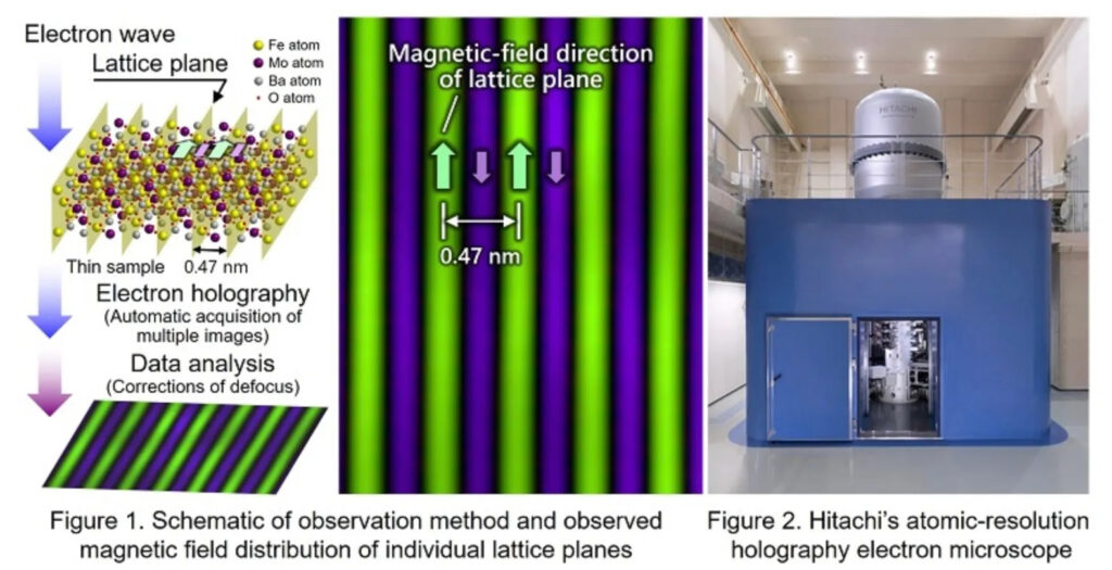
Hitachi, Ltd., Kyushu University, RIKEN, and HREM Research Inc. (HREM) have announced the world’s first observation of magnetic fields of individual lattice planes.*1
Accordingly, the fate became possible after using Hitachi’s atomic-resolution holography electron microscope. Furthermore, with a method enabling magnetic field observation of samples with uneven structures and compositions (non-uniform samples)*2. This include such as magnetic multilayer films, which have been difficult to observe so far, in collaboration with National Institute of Advanced Industrial Science and Technology (AIST) and National Institute for Materials Science (NIMS).
The observation has been made possible by developing a technology with a higher degree of electron-holography precision. Also, with an automated post-image-capture focus correction. For that reason, it is now possible to observe magnetic fields of the atomic-layer level at local boundaries between materials (interfaces). This greatly affects the physical characteristics of materials that include non-uniform samples and characteristics of electronic devices.
In the future, Hitachi will contribute to the advancement of fundamental science by elucidating magnetic phenomena*3 occurring at the atomic-layer level and realization of a carbon-neutral society. Particularly, by developing high-performance magnets and highly functional materials used in electrification for decarbonization. At the same time, energy-saving devices for reducing total energy usage required in our daily life.
Background of the Research
The need for electronic devices and motors are growing in variety of applications. This include mobile phones, personal computers, cars, trains, and power plants.
Moreover, atoms, the smallest unit of matter, and the behavior of electrons, determine many of those functions and performances. As such, to develop new functions and improve performance, there was a need for a technology enabling the ultra-high-resolution observation of matter at an atomic level.
Since 1966, Hitachi has been developing the holography electron microscope as an instrument for the direct observation of electric and magnetic fields in extremely small regions, and in 2014, developed an atomic-resolution holography electron microscope with the support of the FIRST program (Figure 2). In 2017, Hitachi and RIKEN achieved a resolution of less than 1 nm,*5 which enables magnetic-field observation of a few atomic layers.*6 However, to achieve an even higher resolution, there were problems regarding improvement of microscope precision and correction of minute defocusing that occurs when capturing images.
Thus, the collaborative research team solved these problems and developed a technology for realizing magnetic field observation of individual lattice planes for non-uniform samples such as magnetic multilayer films, which have been difficult to observe so far.
The main features of the developed technology
(1) Technology for automated acquisition of large quantities of images for improving precision in electron holography
The precision of electron holography is increased by increasing the number of acquired image data. A technology for automated acquisition of more than 10,000 images over about 8.5 hours while sustaining ultra-high-resolution has been developed by adding automated control and tuning of the microscope during data acquisition and speeding up the imaging based on technology developed in 2017 for precisely separating electric field data and magnetic field data from the result of electron holography observation.
(2) Technology for digital aberration correction that automatically corrects minute defocusing
To obtain high resolution, a technology to correct minute defocusing that remains in observed data is necessary. In addition, the idea of post-image-capture correction of aberrations is exactly the same as that. This motivated Dr. Dennis Gabor to invent electron holography in 1948.
To date, however, there has been no technology for automated correction. In this research, automated correction was successful because of an original algorithm that reduced the impact of noises contained in the experimental data. Specifically, by applying the technique, which corrected defocusing by analyzing electron waves reconstructed from a focus series,*7 to the electron holography.
The developed technology has been applied to the atomic-resolution holography electron microscope to observe magnetic materials (Ba2FeMoO6) with magnetic fields of different strength and directions in each atomic layer. Thus, this has been used to successfully observe magnetic fields of individual lattice planes in the material at the resolution of 0.47 nm, which upon comparing the experimental results with the simulation results was concluded to be the highest in the world*8 for a method that enables observation of uneven samples.
Using this technology, detailed observation of the relationship between interface structures and magnetic fields in devices and materials has become possible, and the development of highly functional materials and energy-saving devices to realize a carbon-neutral society will likely accelerate.
Furthermore, supported by the Project for Promoting Public Utilization of Advanced Research Infrastructure of the Ministry of Education, Culture, Sports, Science and Technology, Japan (MEXT), the atomic-resolution holography electron microscope will be used by various parties. That is, to contribute to the advancement of science and technology in a wide range of fields from fundamental physics to advanced devices.
Notes:
*1 Atoms are the smallest stable particles which form objects. Objects are formed when atoms arranged in 3D. The two-dimensional arrangement of atoms in objects is called a “layer” or “plane.” A “lattice plane” is a structure in which atoms are orderly arranged on a two-dimensional plane in an object.
*2 Here, non-uniform samples are defined not only as samples with random structures such as amorphous but also as samples with different structures and compositions in a periodic structure.
*3 There are Malozemoff’s random field model, which treats magnetic fields of individual small areas as random models and assumes an average magnetic field in case interfaces have non-orderly arranged magnetic atom layers; and magnetic Friedel oscillation, in which atomic layers of non-magnetic and magnetic areas have variation in magnetic field strength in each atomic layer and are different from the magnetic field which has uniform state inside.
*4 Toshiaki Tanigaki, Tetsuya Akashi, Takaho Yoshida, Ken Harada, Kazuo Ishizuka, Masahiko Ichimura, Kazutaka Mitsuishi, Yasuhide Tomioka, Xiuzhen Yu, Daisuke Shindo, Yoshinori Tokura, Yasukazu Murakami, and Hiroyuki Shinada “Electron Holography Observation of Individual Ferrimagnetic Lattice Planes”, Nature, 2024, doi: 10.1038/s41586-024-07673-w
*5 Nanometer (nm): 1nm is equal to one billionth (10-9) of a meter.
*7 T. Tamura, Y. Kimura, and Y. Takai “Development of a real-time wave field reconstruction TEM system (I): incorporation of an auto focus tracking system”, Microscopy, 66, 172-181 (2017).
*8 Based on research by Hitachi in July 2024. Here, the resolution in magnetic field observation is defined as the minimum distance available to differentiate magnetic fields pointing in the same direction.
- Share: