ASIA ELECTRONICS INDUSTRYYOUR WINDOW TO SMART MANUFACTURING
SCREEN Pitches New Direct Imaging System for PCBs
SCREEN PE Solutions Co., Ltd. has released Ledia Qs, a newly developed high-definition direct imaging system that supports package boards.
Demand for semiconductor devices, particularly at datacenters, has grown globally in recent years. Particularly, the widespread adoption of 5G and IoT infrastructure and the development of new technological domains like generative AI propel this trend.
The printed circuit board industry (PCB) is no exception. Accordingly, investment in the high-end circuit board segment, with a particular focus on package boards with semiconductor devices, will continue.
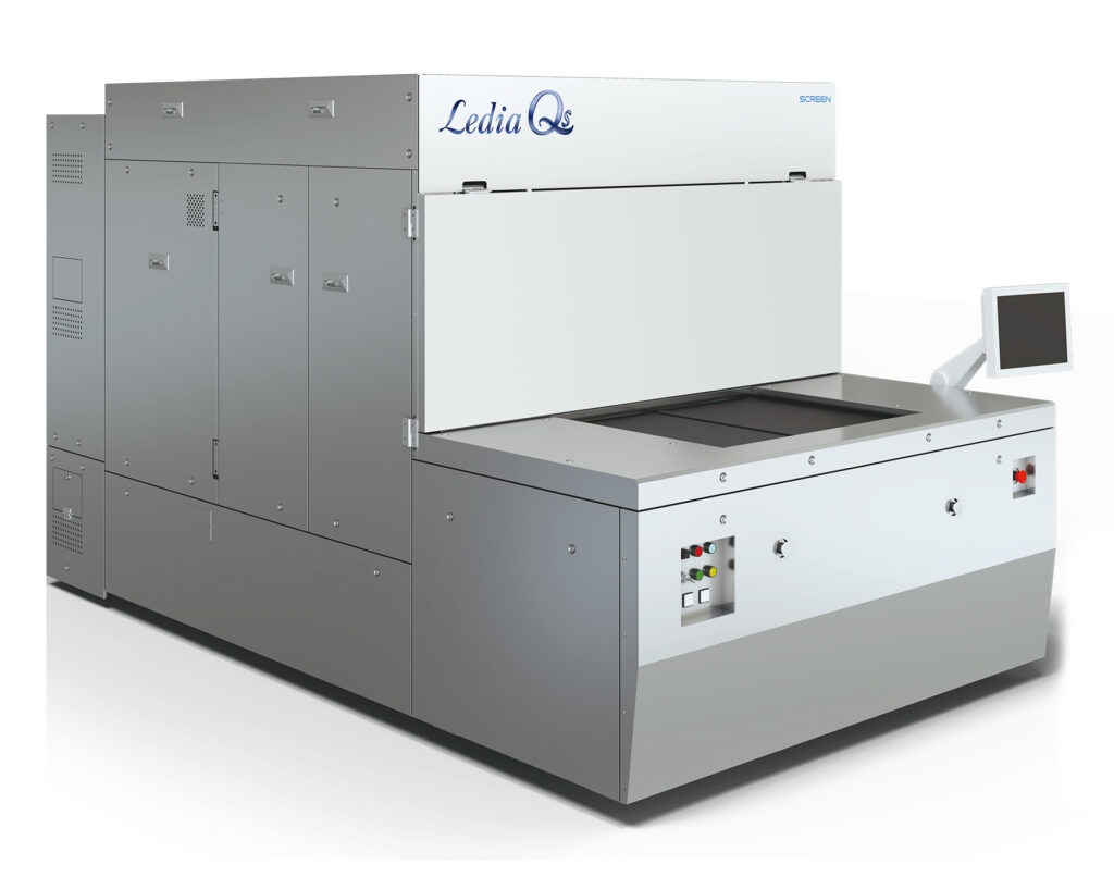
Combines High Image Quality, Stable Image Positioning
The adoption of stepper and other technology in solder resist exposure processes for high-end circuit boards has risen to date. However, the introduction of direct imaging systems capable of satisfying increasingly stringent requirements in areas like positioning accuracy, resolution, and convenience has been much anticipated.
Mainly, the Ledia Qs, a new model in the Ledia Series, developed by SCREEN satisfied these industry needs. The new system adds technology developed for the Ledia 8F, which was announced last year, to SCREEN’s proprietary exposure head, which offers the highest resolution of any broad-wavelength exposure system in the industry. As a result, it can deliver a sophisticated combination of high imaging quality and stable image positioning accuracy.
By expanding the Ledia Series, SCREEN will accelerate its business in the PCB market, which continues to grow. Also, it can contribute to the development of the electronic device industry going forward by meeting a variety of needs.
-12 July 2024-
- Share: