ASIA ELECTRONICS INDUSTRYYOUR WINDOW TO SMART MANUFACTURING
Canon Offers Diverse Portfolio of i-line Stepper
Canon Inc. deploys a broad array of products for semiconductor processes. These range from the manufacture of devices to packaging boards. Particularly, the company offers a rich lineup of i-line stepper systems that meet the miniaturization of wirings and diversification of printed circuit boards from the front-end to advanced back-end processes.
Mainly, Canon handles several types of steppers, including KrF scanners and nanoimprint lithography steppers. Among them, the i-line stepper systems offer a more competitive advantage in the market.
Specifically, FPA-5550iZ2 features upgraded throughput and high resolution as a high-productivity model. It exhibits its power when used in large-scale plants that produce memories and image sensors using primarily 12-inch wafers. Also, FPA-3030i5a supports substrates 8-inch or smaller in diameter and special substrates. It manufactures power and radio frequency (RF) devices.
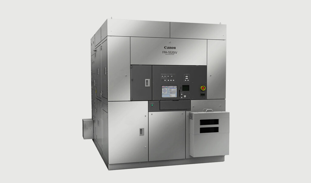
As a stepper for back-end processes, FPA-5520iV for advanced packaging features a wide field and a deep depth of focus to meet thick-film resists. Meanwhile, the design of FPA-8000iW suits panel-level packaging. It manufactures square substrates measuring about 500×500mm. Mainly, these steppers for back-end processes are used for the imaging of artificial intelligence (AI) chips and application processors for smartphones.
Generally, Canon’s i-line steppers meet the diversification of substrates. Mainly, they cover from 2-inch wafers, such as gallium nitride (GaN) wafers, to 12-inch panels, such as fan-out wafer level packaging (FOWLP) substrates. They also cover substrates with redistribution layers formed on resin.
Multi-Platform Strategy
Specifically, Canon sets forth a multi-platform strategy. Under which, the company makes optimal proposals by combining various units that constitute steppers, including main body system, projection lens, and alignment mechanism that meet various substrate sizes. For example, when an alignment mark, which is normally on the surface, is on the back side, checking the mark used for positioning using an optical microscope is not possible. In such a case, Canon proposes a system equipped with an infrared scope. Specifically, it captures the mark by passing through the silicon. This way, the company meets diverse needs.
- Share: