ASIA ELECTRONICS INDUSTRYYOUR WINDOW TO SMART MANUFACTURING
NEG's New Tech Results in Breakthrough GC Core
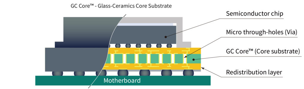
Nippon Electric Glass Co., Ltd. has developed a glass-ceramics core substrate (GC Core™), which has promising potential for use in next-generation semiconductor packages.
Development background
Recently, there has been growing demand for data centers and the increase in data traffic due to the spread of technologies. Among them is generative artificial intelligence. For that reason, there has been a demand for higher-performance and lower-power semiconductors used in the infrastructure that supports these technologies.
To improve the performance of semiconductors, it is essential to miniaturize circuits, develop chiplets,*1 and increase the size of substrates. However, conventional plastic core substrates*2 make it difficult to miniaturize circuits. Moreover, they also have rigidity issues, such as deformation when mounting multiple semiconductor chips or making the substrate larger.
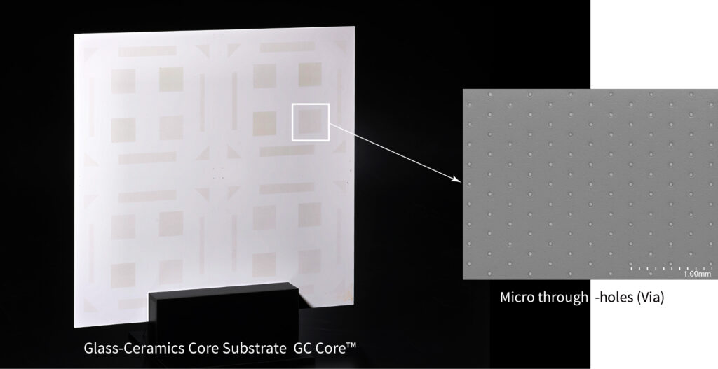
Therefore, progress is being made in developing core substrates made of glass, which has excellent electrical properties, rigidity, and flatness, as a next-generation material to replace plastic core substrates. The GC Core™ that NEG has recently developed is a core substrate made from a composite of glass powder and ceramic powder. In addition to the properties of a core substrate made of glass, the new material offers the advantage of being easy to machine when making micro through-holes.
Features of GC Core™ developed by Nippon Electric Glass
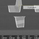
(1) Capable of being drilled with a CO2 laser
Micro through-holes need to be formed in the core substrate to electrically connect the fine metal wiring formed on the front and back sides.
High-speed & crack-free
When drilling holes in ordinary glass substrates with a CO2 laser, a certain percentage of them will develop cracks, which can lead to breakage of the substrate. The GC Core™ has the properties of ceramics*3 as well. Therefore, enabling high-speed, crack-free drilling.
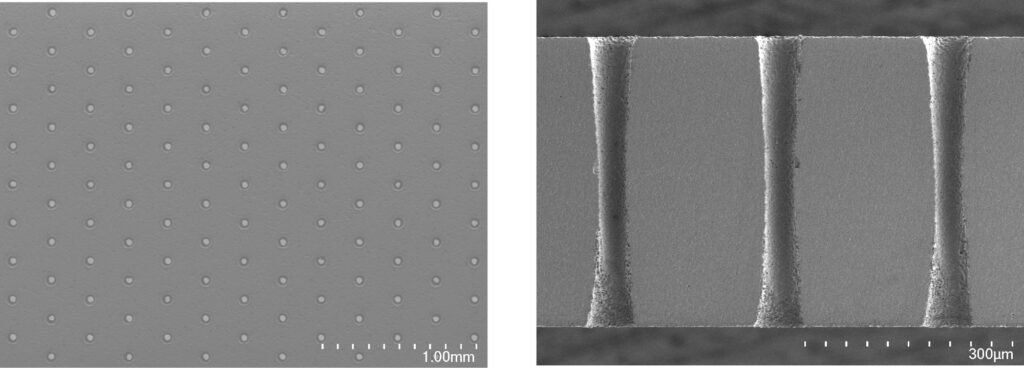
Economical and expected to reduce mass production costs
When drilling holes in ordinary glass substrates, the most common method is to use laser modification and etching to create holes to avoid cracks, but this method is technically difficult and requires capital investment.
The GC Core™ is economical because the holes can be made using a widely used CO2 laser machines. Hence, the company expects to reduce mass production costs.
(2) Low dielectric constant and loss tangent
The glass-ceramic material uses low temperature co-fired ceramics (LTCC), a material developed exclusively by NEG. This material has a low dielectric constant and loss tangent*4 and reduces signal delay and dielectric loss.
(3) Thin substrates available
The GC Core™ is stronger than glass substrates, allowing for thinner substrates, contributing to thinner semiconductors. In addition, because it is less likely to break, it offers improved ease of handling during the semiconductor package production process.
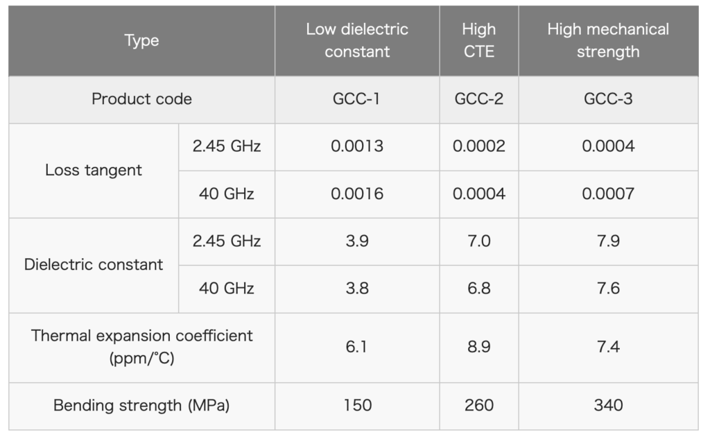
(4) Easily change specifications to meet customers’ needs
The properties of the GC Core™ which depend on the composition and compounding ratio of glass and ceramics can be tailored to your needs. In addition to low-dielectric-constant types with excellent dielectric properties, NEG also offers high-expansion types that match the thermal expansion of plastic substrates and high-strength types. Thus, making it possible to develop substrates that can be used for a wide range of applications.
Future Plans
NEG has become successful in developing a 300mm-square substrate. Currently, the company is working on developing of an enlarged substrate of up to 515×510mm by the end of 2024. In fact, the company featured the 300mm-square substrate at the JPCA Show 2024 held at Tokyo Big Sight last June 12 to 14.
Notes:
*1. Chiplets: An advanced semiconductor packaging technology that densely mounts multiple semiconductor chips with different functions on a single substrate, improving processing speed.
*2. Core substrate: The substrate material that serves as the base on which semiconductor chips are mounted.
*3. Properties of ceramics: Ceramics have a crystalline structure. The atoms and ions within the crystal are strongly bonded together. Therefore, ceramics are relatively strong against external forces in terms of deformation and cracks.
*4. Loss tangent: A measure of energy when a dielectric substance is polarized. The smaller the loss tangent, the lower the conversion of electromagnetic energy into heat, and as a result attenuation of signals is reduced.
24 July 2024
- Share: