ASIA ELECTRONICS INDUSTRYYOUR WINDOW TO SMART MANUFACTURING
Digital Lithography Offers Novel Chip Patterning Approach
For years, increases in semiconductor performance were achieved by shrinking device features using masked-based optical photolithography with shorter and shorter wavelengths, and then packing more and more of the smaller printed features into 2D monolithic chips. As lithographic scaling has slowed down due to technical and cost challenges, the semiconductor industry has turned to heterogeneous integration – the manufacturing, vertical assembly and packaging of multiple different dies into a single package – to enable continuous improvements in device performance while minimizing increases in packaging footprint. However, this move to heterogeneous integration has led to greater package complexity, as well as in the number of package options available – in turn driving the need for greater design flexibility and the ability to adopt both die-level and wafer-level designs simultaneously in back-end lithography (Figure 1).
Lithography requirements are not just changing in the back-end in advanced packaging. Wafer probe cards play a crucial role in semiconductor testing by enabling the identification of defects in devices while still in wafer form prior to assembly and packaging processes. Advanced wafer probe cards incorporate micro-electro-mechanical systems (MEMS) technology to enable micron-level precision contact with power connections and I/Os on ICs. This precision makes MEMS probes ideal for fine-pitch requirements that are needed for testing increasingly sophisticated devices. However, MEMS-based fine-pitch probe cards pose challenges for traditional mask-based lithography solutions due to their multiple lithographic steps as well as their complex product mix, which drives up mask/reticle overhead costs.
In fan-out wafer-level packaging (FO WLP) and fine pitch probe card manufacturing, interconnect formation is a cost-demanding process (Figure 2). First, the VIA (polymer1) is patterned by the steps of coating, exposure, development, UV cure and post cure bake. Afterwards, the redistribution layer/RDL (polymer2) for the METAL2 layer is patterned by coating, exposure, development, UV cure, post UV cure and descum.

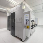
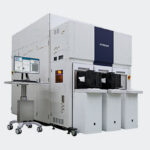
Traditional mask-based lithography solutions are no longer practical for many advanced packaging and wafer probe card applications, especially those requiring fast prototyping and testing of new product designs or highly customized solutions, where the cost and time needed for producing, testing and reworking a large volume of mask sets can quickly add up. EV Group has introduced a maskless exposure technology, called LITHOSCALE®, that represents a novel, digital patterning approach that enables new application development beyond what is possible with traditional, mask-based exposure systems. The technology features real-time data processing and patterning, advanced distortion function, die-shift compensation, high autofocus, high in-focus range, and top-side and bottom-side multipoint alignment capabilities.
LITHOSCALE tackles the demand for design flexibility, high scalability and productivity. Its mask-free approach eliminates mask-related consumables, while the tunable solid-state laser exposure source is designed for high redundancy and long life-time stability with virtually no maintenance and no re-calibration required. Powerful digital processing enables real-time data transfer and immediate exposure – avoiding hours of setup time for each digital mask layout as needed by other maskless lithography systems. The system is capable of individual die processing, while fast full-field positioning and dynamic alignment enable high scalability for a range of substrate sizes and shapes. The result is a highly versatile maskless lithography platform geared for a variety of micro-electronic production applications.
Advanced Distortion Functionality
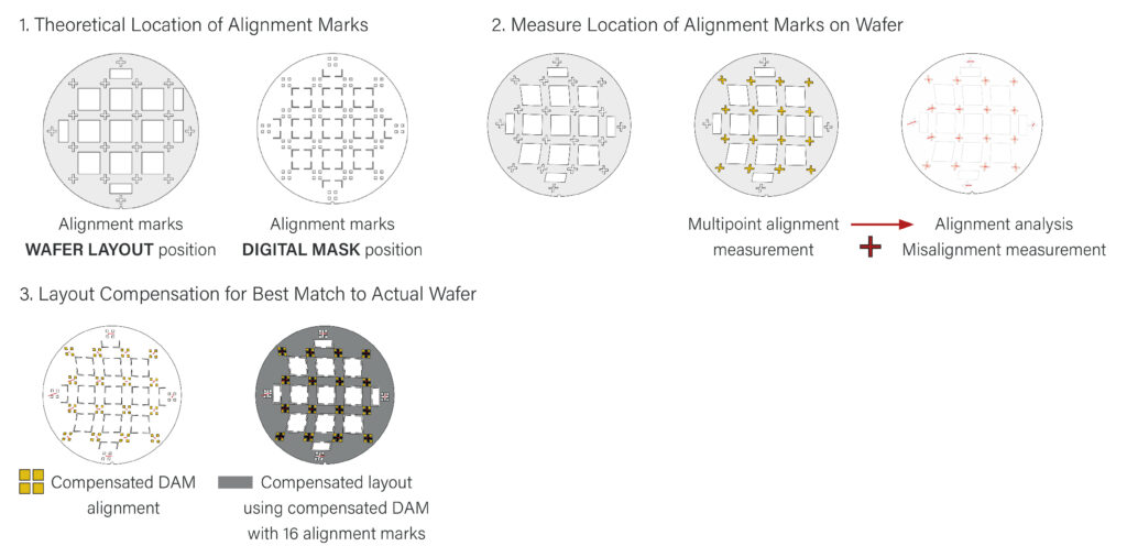
LITHOSCALE’s advanced distortion function works by first determining the theoretical locations of the alignment marks. After alignment marks determine wafer layout positioning, the alignment marks for digital mask positioning follows. Global (4 points) and multipoint (16 points) alignment features are available. The location of the alignment marks on the wafer is measured. The layout is compensated for best match to actual wafer. The system provides the distortion of GDSII data in real time without delay. Data is distorted based on alignment information and stage distortion information to compensate for misalignment. The workflow is illustrated in Figure 3.
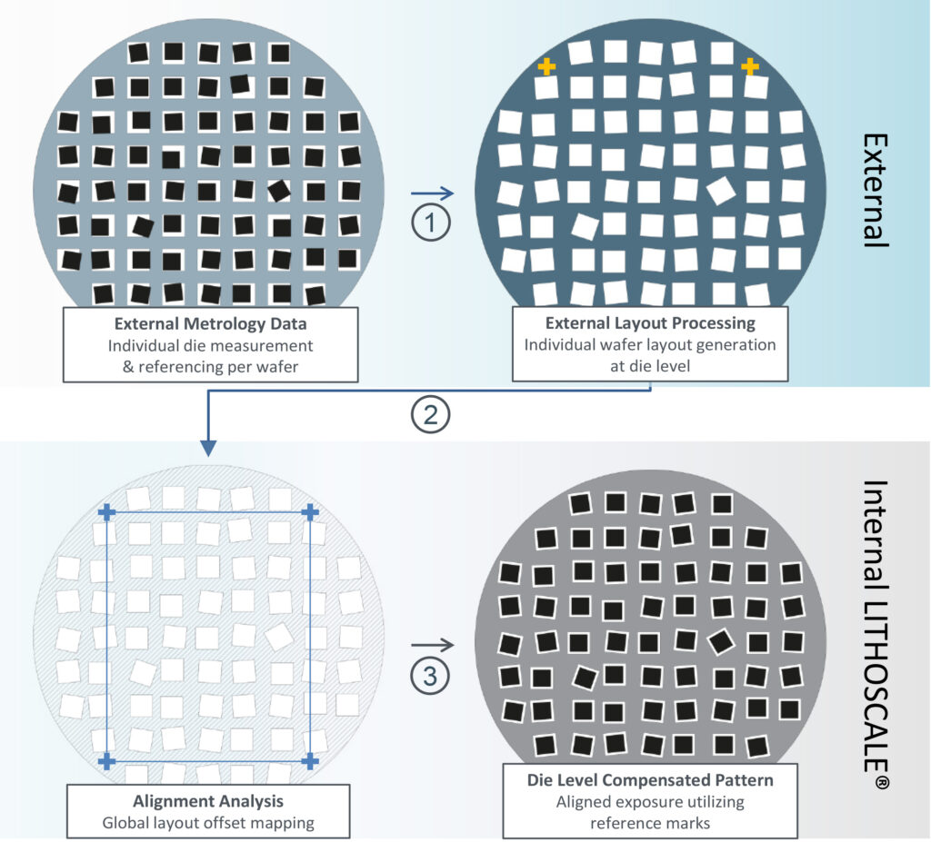
Advanced distortion functionality is applied on the die level, where active compensation and re-routing results strictly rely on external metrology data. Distortion compensation algorithms include mathematical correction of rotation, scale, shear, and translation (shift). For die-placement-error compensation, the model limits distortion within the dies to the rigid body of the die, typically represented in two (external) alignment points per die. Due to the immediacy of the conversion processes, the dynamic binary pattern generation complements externally required metrology data of each die individually per substrate just before the exposure to compensate for overlay/positioning errors caused by handling or pre-processing excluding potential thermal influences. A simplified data integrity flow of die level compensation is visualized on Figure 4.
LITHOSCALE’s software system architectures accomplish real-time exposure. There is no additional time needed for layout conversion/calculation. There is no impact of layout flexibility on the wafer throughput. Data processing does not limit the throughput. The multi-head configuration enables parallel wafer processing. The minimum achieved resolution is <2µm line and space (L/S). The maintenance-free laser light source is part of the LITHOSCALE system. Operating with dual wavelengths, 375 nm and 405 nm, the system can process a broad range of materials, including thin and thick resists, dielectric materials, and colored resists. The broad process windows matrix setup ensures efficient process evaluation.
Maskless Exposure for UHD FO WLP for 5G, AI and HPC
The application of steppers in next-generation packaging technology faces several challenges. Accurate reconstitution of the wafers is a key parameter in integrating dies from various wafer fabs in multi-die solutions. Steppers and other mask-based patterning systems struggle to cope with inaccuracies from die-placement and die-shift variations caused by over-molding. The reticle size and optics dimensions of static exposure systems limit the exposure area. This is particularly challenging in large die interposer fabrications, where stich-lines and/or mismatches overlap regions of reticle exposure field, which can affect the electrical properties within the redistribution layer (RDL). The ability to generate a homogenous pattern for interposers exceeding current reticle size is crucial for advanced devices needed for complex layouts, such as advanced graphic processing, 5G, artificial intelligence (AI) and high-performance computing (HPC).
LITHOSCALE overcomes the difficulties caused by steppers in advanced packages. Resolution and best patterning conditions of the dielectric materials were studied with LITHOSCALE. Both negative-tone PI and positive-tone PBO formed vias with high resolution. The minimum resolution of the PI layer scales well with stress buffer layer thickness for all wavelengths studied. The effect on resolution for PBO is minimal. PBO requires a higher dose for thicker layers and resolution of PI is less dose dependent. The proven contact via with a bottom opening down to 2µm can significantly improve scaling and interconnect density enhancement.
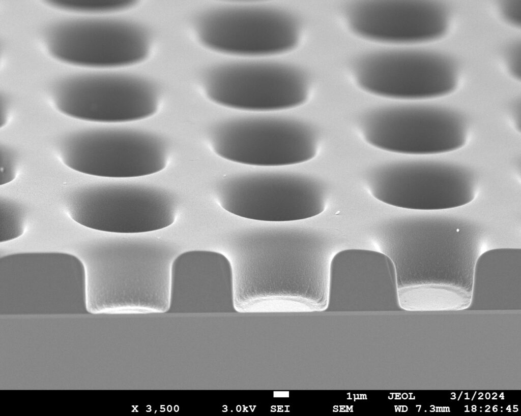
In a new study, LITHOSCALE was employed to evaluate newly developed high-resolution PI dielectrics on both silicon- and copper-plated wafers. The results reveal that VIA profiles even less than 5µm were achieved when qualifying LITHOSCALE for ultra-high-density (UHD) FO WLP applications. The SEM cross section of the patterned structure is illustrated in Figure 5. The exposure technology achieved the steep profiles in the PI dielectric material required for further seamless integration processes and for achieving the high electrical properties required for AI and HPC devices.
Maskless Exposure for Fine-pitch Probe Cards
Market requirements for fine-pitch probe cards involve numerous layout designs that are unique for each new product to be tested. As a result, many masks in production are necessary, which contribute to high costs. Unique benefits of LITHOSCALE in probe card applications include supporting immediate patterning after design release, and the ability to quickly react on end-user requests/needs and design changes. A flawless processing of the positive-tone resists and dielectric materials for fine-pitch probe cards applied in advanced NAND and DRAM memory devices is enabled (Figure 6). A concept of double-layer exposure is economically beneficial since the lithographic steps can be reduced when patterning the multiple RDL structures. For the interconnect formation in fine-pitch probe cards as well as FO WLP, LITHOSCALE represents a convenient and cost-effective solution vs. mask-based systems.
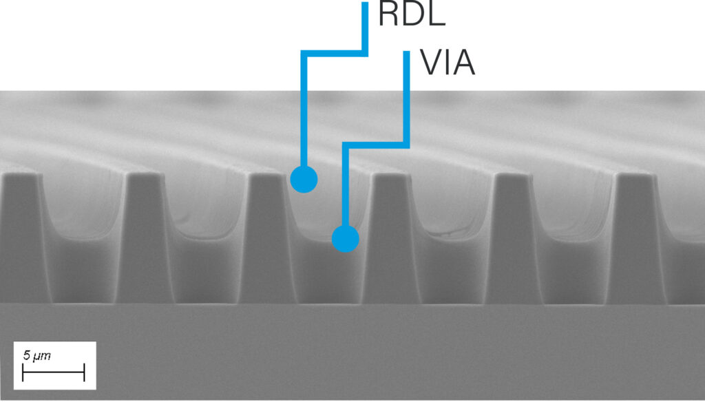
The patterned RDL traces via 5μm; opening 3μm (Source: EV Group)
Summary
The novel LITHOSCALE maskless exposure lithography system with its unique combination of mechatronics, optics and advanced software capabilities accomplishes patterning <2µm L/S, by efficient digital mask processing and real-time patterning. Its distortion compensation, die-shift compensation, and alignment <1 µm is crucial for overcoming the limitations of mask-based patterning technologies in next-generation advanced packaging devices. The technology is positioned in a variety of industries, from automotive, MEMS and photonics, to advanced packaging, fine-pitch probe cards and more. The future of lithography technology is truly digital.
About the Authors
Ksenija Varga is a business development manager at EV Group, with a particular focus on developing new applications for maskless exposure technology. The launch and technical positioning of new lithography equipment is also part of her role. Additionally, Ksenija is involved in EVG’s strategic technology roadmap, with a particular focus on the future development of EVG’s lithography portfolio. Ksenija holds a doctorate in chemistry (Dr. rer. nat.) from the University of Innsbruck in Austria.
Thomas Uhrmann, PhD, is Director of Business Development at EV Group, Austria. He is responsible for overseeing all aspects of EVG’s worldwide business development. Previously, he was business development manager for 3D and advanced packaging as well as compound semiconductors and Si-based power devices at EV Group. He holds an engineering degree in mechatronics from the University of Applied Sciences in Regensburg and a doctorate in semiconductor physics from the Vienna University of Technology (TU Wien).
-04 September 2024-
- Share: