ASIA ELECTRONICS INDUSTRYYOUR WINDOW TO SMART MANUFACTURING
FUJIFILM to Expand IC Material Business with New Funds
FUJIFILM Corporation has announced an investment of 20 billion yen (US$139 million) in its semiconductor materials business. Primarily, the investment aims to further strengthen its facilities for the development, production and quality evaluation of advanced semiconductor materials in Shizuoka and Oita, Japan.
Driven by high-speed, high-capacity communications through 5G/6G, the expansion of autonomous driving, and the spread of AI and the metaverse, demand for semiconductors is expected to increase and their performance is projected to advance as well. Consequently, ensuring a stable supply of higher quality and higher performance semiconductor materials for the semiconductor manufacturing process has become increasingly critical.
Mainly, FUJIFILM offers semiconductor materials used in wafer processing to post processing in semiconductor manufacturing. These include photoresists*1, photolithography-related materials*2, CMP slurries*3, post-CMP cleaners*4, thin-film chemicals*5 and polyimides*6, as well as WAVE CONTROL MOSAIC™*7, which includes color filter materials for image sensors. In addition to its extensive product lineup covering almost the entire range of semiconductor manufacturing processes, from leading-edge to legacy semiconductors, Fujifilm is committed to solving customers’ issues by providing one-stop solutions that leverage its global supply structure and advanced R&D capabilities. At the same time, the company is making aggressive capital investments in production facilities globally. As a result, it is expanding production capacity of semiconductor materials.
Strengthen Sites in Shizuoka and Oita
FUJIFILM Electronic Materials Co. Ltd. is the core company that leads Fujifilm’s semiconductor materials business. Particularly, it will strengthen and expand its sites in Shizuoka and Oita. This effort aims to enhance the development, production, and quality assurance of advanced semiconductor materials.
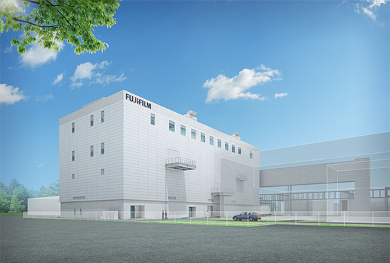
At the Shizuoka site, FUJIFILM Electronic Materials invests approximately 13 billion yen (US$90.3 million) to construct a new building. It aims to strengthen the development, production and quality evaluation functions for advanced photoresists, including photoresists for extreme ultraviolet lithography(EUV), and WAVE CONTROL MOSAIC™. Specifically, the new building will be equipped with a clean room and state-of-the-art inspection equipment. With the new facility, the company will further speed up development, expand production capacity, and enhance its quality evaluation systems.
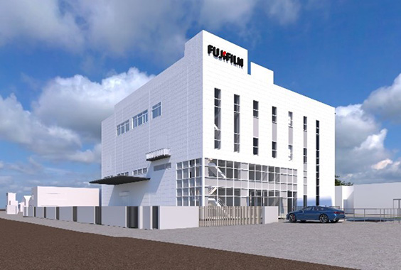
Meanwhile, at the Oita site, FUJIFILM Electronic Materials invests approximately 7 billion yen (US$48.7 million). Specifically, it will construct a new building, acquiring land adjacent to the existing site. It will introduce additional production equipment and inspection devices for post-CMP cleaners. Specifically, they are key materials in the semiconductor manufacturing process. Thus, this will expand the production capacity at the Oita site by approximately 40%.
Particularly, post-CMP cleaners are used in the process of uniformly flattening the surface of semiconductors. Post-CMP cleaners are used after polishing with CMP slurry to remove particles, minute metal fragments and organic residues while protecting the metal surface. The market is expected to grow at an annual rate of 9%*8.
Further, Fujifilm will expand its business as the equipment enhancement enables more stable and rapid supply of post-CMP cleaners. In addition, by making the most of its strength in being able to propose post-CMP cleaners in combination with CMP slurry to customers, it will enhance its contribution to solving the customers’ issues and further improvements in semiconductor performance.
The new building at the Shizuoka site is scheduled to begin operations in the fall of 2025. Meanwhile, the new building at the Oita site is scheduled to begin operations in the spring of 2026.
Fujifilm will continue to contribute to the further development of the semiconductor industry. Particularly, it will accelerate the development and the stable supply of semiconductor materials that cover a wide range of products, from leading-edge to legacy semiconductors.
* WAVE CONTROL MOSAIC is a registered trademark or trademark of FUJIFILM Corporation.
*1 Material used to coat wafer substrate when circuit patterns are drawn in the process of semiconductor manufacturing
*2 Development solutions, cleaners and other materials used in the photolithography process of semiconductor manufacturing
*3 A polisher for evenly levelling semiconductor surface, which contains a mixture of wires and insulation films of varying hardness.
*4 Cleaners used after polishing with CMP slurry to remove particles, minute metal fragments and organic residues while protecting the metal surface
*5 Materials for forming low-dielectric insulation films
*6 A material with strong heat resistance and insulation properties, used for forming semiconductors’ protective films and rewiring layer
*7 General term referring to a group of functional materials for controlling electromagnetic light waves in a broad range of wavelengths, including photosensitive color materials for manufacturing color filters for image sensors such as CMOS sensors, used in digital cameras and smartphones
*8 Electronic Materials Forecasting Report 2023 by the U.S. research company “Linx”
-02 October 2024-
- Share: