ASIA ELECTRONICS INDUSTRYYOUR WINDOW TO SMART MANUFACTURING
SEDEX 2021 Opens in Seoul, Charting Out Roadmap for New Chip Solutions
SEDEX 2021 open today at COEX, inviting 237 domestic and foreign players in the global semiconductor manufacturing ecosystem.
The 3-day annualized trade show is to run through Oct. 29, displaying a wide variety of cutting-edge chip solutions as well as top-of-line manufacturing equipment and innovative chemical compound materials.
The exhibition is being held at a time when digital transformation is speeding across all industries and societies to prepare themselves for the post-COVID-19 pandemic era, creating tones of new data-hungry applications like online conferences and live video streaming
At a keynote speech held online, Lee Jung Bae, CEO with Samsung Electronics’ memory business unit, said, “The COVID-19-forced social-distancing phenomenon has been unearthing a wealth of new data-hungry applications like AI and autonomous driving, Metaverse, and human robots, offering new market opportunities for chip makers.”
“Yet, it also necessarily posing challenges, as chip makers are struggling to ramp with ever finer chip process technologies, which can enable them to embed more of transistors into silicon to get wider data bandwidth,” he added.
True enough, memory chip makers like Samsung Electronics are now finding it increasingly ough to go below 14nm chip process technology, seeing their ramp-up to below 14nm technology dragging feet. Meanwhile, logic chip makers are echoing that it would take longer time than expected to attain 1nm chip process technology. When it comes to NAND flash memory chips, it is getting tough and tougher to vertically stack up transistor cells as high 1,000 layers.
So, CEO Lee calls for chip makers, equipment makers, and materials makers to all cooperate to tackle these challenges.
He also suggested anther way out, calling for innovations in chip structure as well as packaging technologies.
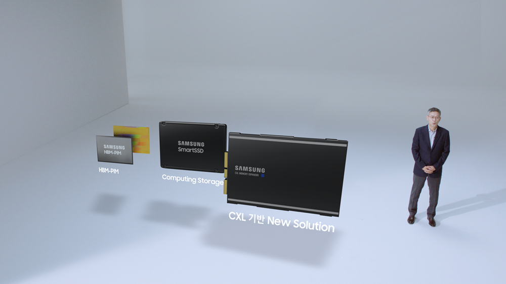
One prime example now in progress is what’s called as PIM, or processor in memory chip solutions, which embed AI processor and memory chip together in a silicon wafer. The memory-centric processor chip solution is now under development to process massive amounts of data on AI processors, as AI applications are clamoring for more of data feeding to infer, analyze, predict various trends as exactly as possible.
Innovations in the interconnections technologies between chips -memory chips, accelerators, and processors- are also another way around, as it allow tones of data to move back and forth between chips as quickly as possible. A case in point is what’s called as Compute Express Link, or CXL, which is an industry-supported cache-coherent interconnect technology for processors, memory expansion and accelerators. Available now in the 2nd version, the CXL technology maintains memory coherency between CPU memory space and memory on attached devices, allow them to share bandwidth resources for higher performance, reduced software stack complexity, and lower overall system cost. This permits users to simply focus on target workloads as opposed to the redundant memory management hardware in their accelerators.
“In order to process explosions in data traffic as adroitly as possible, we need other breakthrough innovations elsewhere than in chip process technologies,” he stressed
Meanwhile, Samsung Electronics has unveiled a new generation of chip technologies at its booth, including EUV-based 14nano DDR5 DRAM chips, a 200 million pixel, or 200MP CMOS image sensors, GAA, or gate all-around-centric processor chips called as MBCFET, or multi-bridge channel filed effect transistor technology. The MBCFET is one of the most advanced chip-making technologies available now, under which channels are wrapped around a gate from multiple directions.
Designed to be used in applications from low power to high performance, the MBCFET requires cutting-edge innovations in material technology such as nanosheet high-k metals, for example.
SK hynix has also displayed high speed and high bandwidth HBM, or high bandwidth memory chip solutions for AI, Big Data, VR-based metaverse, autonomous driving, and 5G and 6G communications as well as consumer SSDs
Equipment and raw material makers like PSK and Dongjin Semichem of Korea have unveiled PR photo resistor-cleaning machine strippers as well as key raw materials.
Komico, a maker of cleaning and coating equipment, has showcased the latest in its coating and cleaning equipment product line-up.
Shinsung ENG has taken warps off its remote wireless smart monitoring system that can monitor and manage various equipment in the semiconductor cleanroom.
Other equipment and raw materials makers on the scene include MiCo Ceramics, Wonik IPS, and KCTech.
- Share: