ASIA ELECTRONICS INDUSTRYYOUR WINDOW TO SMART MANUFACTURING
Applied Angstrom’s New Atomic Precision Hub Targets AI Chips
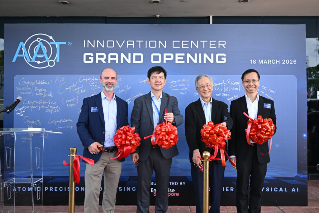
The expanding demand for AI computing has ushered in a new era of angstrom-scale chip manufacturing, which is also propelling a new generation of wafer equipment. For that reason, deep tech startup Applied Angstrom Technology (AAT) opened Wednesday (March 18) its Atomic Precision Innovation Center (APIC) in Singapore, a purpose-built facility focused on angstrom‑scale semiconductor manufacturing equipment.
AAT is positioning APIC squarely at the intersection of advanced process technology and AI-driven hardware demand. The facility integrates Front-End-of-Line (FEOL) equipment design, testing, and production. Thus, enabling AAT to mount complete etch systems under one roof.
Dr Richard Yang, Ph.D., Founder and CEO, Applied Angstrom Technology, said, “By mastering precision at the atomic scale and AI-native design, and with APIC being close to major foundries, suppliers and research partners, we aim to bolster Singapore’s role in deep tech innovation while contributing to the region’s long-term competitiveness in AI hardware.”
Next Frontier Chip Equipment
The opening of AAT’s APIC facility happened at a time the semiconductor industry’s traditional chip manufacturing platforms are reaching physical limits. More powerful and higher density chips require a different and more innovative approach to how they are etched and layered.
AAT’s focus on Atomic Layer Etching (ALE) addresses this challenge by enabling material removal at sub-nanometer resolution—critical for advanced logic, memory, and silicon photonics used in AI infrastructure.
Rather than evolving legacy equipment platforms, AAT is developing clean-sheet, AI-native etch systems designed from the ground up for the Angstrom Era.
“The chips that power AI need equipment that is itself powered by AI,” said Dr. Yang in an interview with AEI.
Rather than iterating on decades-old platform designs, Dr. Yang said AAT is building next-generation equipment from the ground up, powered by agentic AI from day one and accelerated by physical AI for future development.
Dr. Yang, who pioneered ALE and transitioned cryogenic etch to fab scale at Lam Research and Intel, founded AAT in Singapore in 2022
Strengthens Singapore Position in Angstrom Era
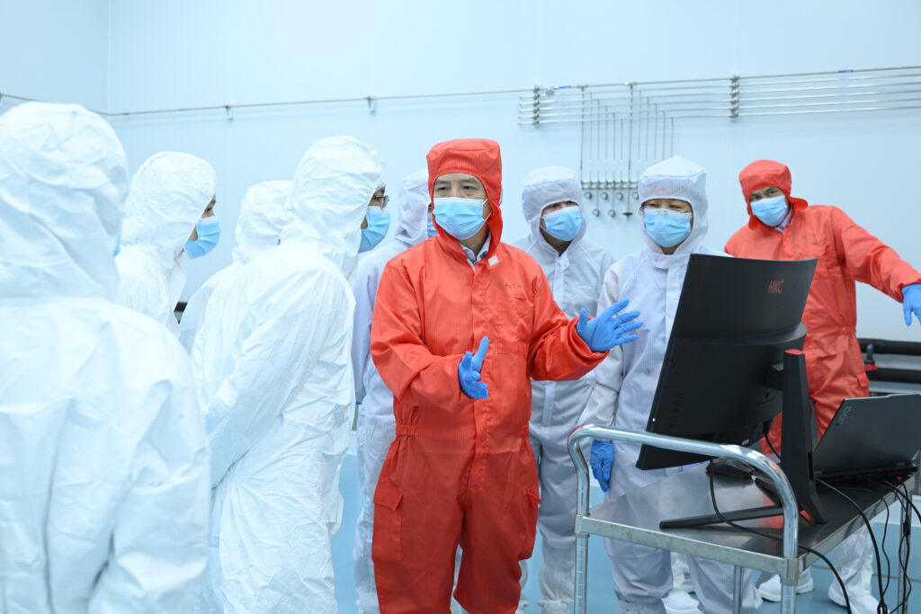
AAT’s new facility in Yishun Industrial Park is within close reach of major semiconductor hubs in Singapore. The 10,000sq.ft center includes a 2,000sq.ft Class 100 (ISO 5) cleanroom.
At full utilization, APIC can support the parallel development of more than three systems and deliver an annual turnaround of eight or more atomic-precision semiconductor systems.
APIC has the support of Enterprise Singapore under the Ministry of Trade and Industry. APIC is backed by investor iGlobe Partners, alongside strategic partner Sioux Technologies, which is collaborating with AAT on AI-native software development.
“The Atomic Precision Innovation Center (APIC) plays an important role in strengthening Singapore’s position as a resilient and diversified semiconductor supply chain hub,” said Mr. Wong Zeng Yi, Assistant Managing Director, Manufacturing, Enterprise Singapore.
19 March 2026
- Share: