ASIA ELECTRONICS INDUSTRYYOUR WINDOW TO SMART MANUFACTURING
Imec to Drive Quantum Scale With EUV Tech
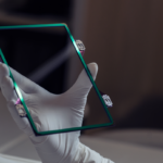
imec has introduced what it describes as the first quantum dot qubit device fabricated using High‑NA EUV lithography, marking a significant step toward scalable quantum computing.
The development, presented at ITF World, underscores how advanced semiconductor manufacturing technologies are beginning to play a central role in the next phase of quantum hardware. According to imec, the device is the first integrated hardware system created using High‑NA EUV lithography—a capability traditionally associated with cutting-edge chip production.
Towards Scalable Quantum Systems
Quantum computing has long promised major gains in tackling complex problems across many industries. However, turning that promise into practical systems depends on scaling up from a small number of qubits to millions that can operate reliably and in coordination.
imec’s latest work addresses this challenge by leveraging silicon quantum dot spin qubits, a platform widely viewed as suitable for industrial scaling. These qubits are compatible with established CMOS semiconductor manufacturing processes, allowing companies to build on existing chipmaking infrastructure rather than creating entirely new production models.
The compatibility means quantum computing could evolve within the current semiconductor ecosystem, potentially reducing cost and time barriers to commercialization.
Precision at Nanoscale
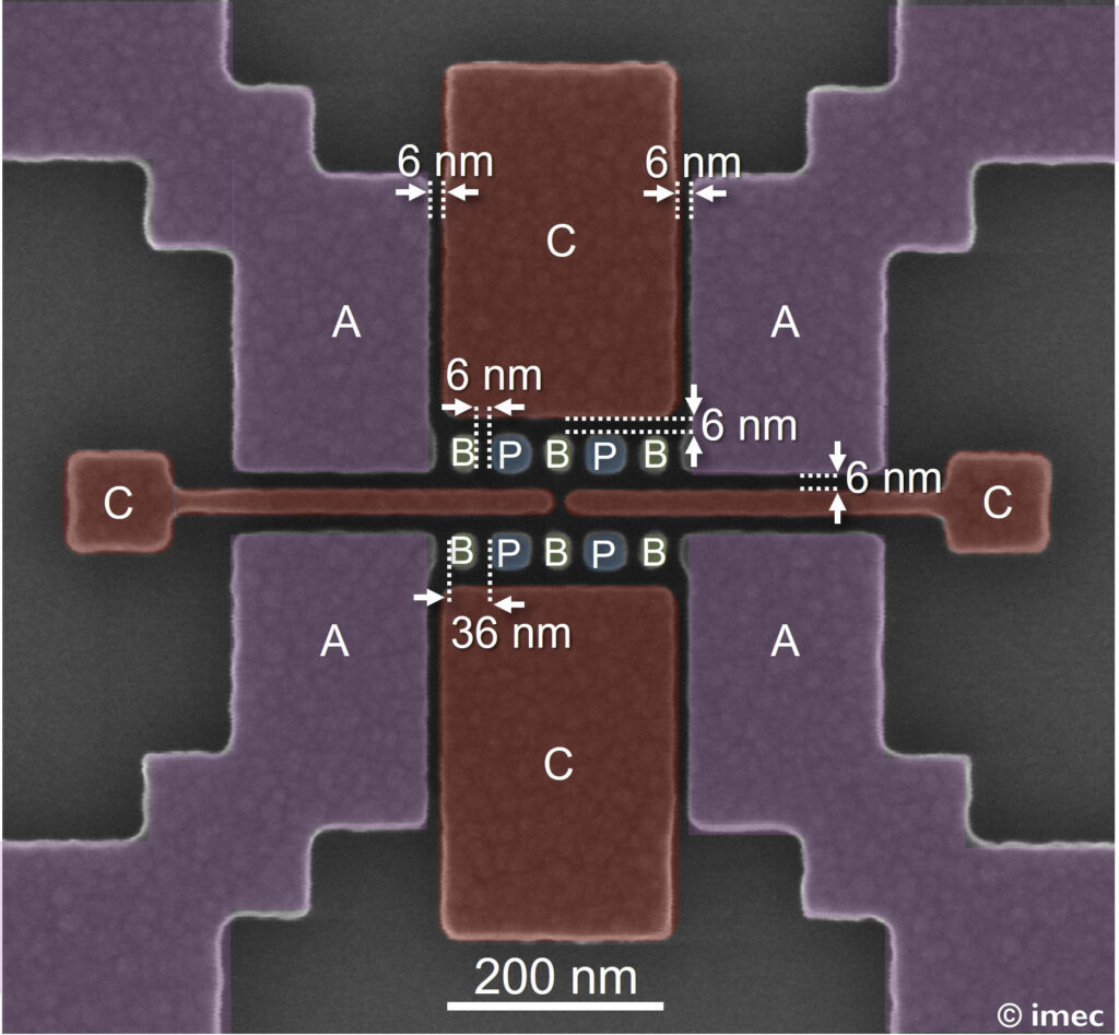
At the core of the breakthrough is the ability to precisely pattern extremely small structures that control qubit behavior. Silicon quantum dot qubits work by trapping electrons in nanoscale regions, using their spin to store information.
To function effectively, these structures must be placed with extreme accuracy. imec reported achieving gaps of around 6nm between critical components—small enough to improve qubit interaction while minimizing interference from the environment.
High-NA EUV lithography played crucial role in this level of precision. This next-generation patterning technique delivers higher resolution than previous systems. By shrinking these gaps, imec demonstrated a functioning network of qubits that can, in principle, be scaled to much higher densities.
Extending Advanced Lithography into Quantum
The demonstration also highlights a broader trend: technologies initially developed for advanced computing chips are increasingly being applied to emerging fields such as quantum computing. imec noted that High‑NA EUV lithography—critical for future memory and logic chips—can also serve as a foundation for next-generation quantum devices.
For businesses, the significance lies less in a single device and more in what it represents: a potential path to industrial-scale quantum hardware. By combining proven semiconductor processes with new quantum architectures, imec’s approach aims to move quantum computing from laboratory experiments toward manufacturable systems.
20 May 2026
- Share: