ASIA ELECTRONICS INDUSTRYYOUR WINDOW TO SMART MANUFACTURING
TSMC, Sony Partner in New IC Fab Joint Venture
Taiwan Semiconductor Manufacturing Company Limited (TSMC) and Sony Semiconductor Solutions Corporation (SSS) have partnered to set up a new subsidiary. Japan Advanced Semiconductor Manufacturing, Inc. (JASM) will initially produce 22nm and 28nm processes.
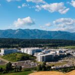
The alliance targets the new foundry service, which will rise in Japan’s Kumamoto, to address strong global market demand for specialty technologies. SSS will participate as minority shareholder.
A statement released by TSMC and SSS pegged the initial capital expenditure at US$7 billion with the Japanese government expressed its strong support to the project.
Support to New IC Fab
The construction of JASM will begin in 2022 and production will start by the end of 2024. The new foundry targets to employ 1,500 high-tech professional jobs with monthly production capacity of 45,000 12-inch wafers.
Under definitive agreements reached between TSMC and SSS, SSS plans to make an equity investment in JASM of approximately US$500 million, which will represent a less than 20 percent equity stake in JASM. The closing of the transaction between TSMC and SSS is subject to customary closing conditions.
“The digital transformation of more and more aspects of human lives is creating incredible opportunities for our customers, and they rely on our specialty processes that bridge digital life and real life,” said Dr. CC Wei, Chief Executive Officer of TSMC. “We are pleased to have the support of a leading player and our long-time customer, Sony, to supply the market with an all-new fab in Japan. (We) also are excited at the opportunity to bring more Japanese talent into TSMC’s global family.”
Meanwhile, Terushi Shimizu, President and Chief Executive Officer of SSS said the partnership with TSMC will contribute to securing a stable supply of logic wafers not only for the two companies but also for the overall industry.
“We believe that further strengthening and deepening our partnership with TSMC, which has the world’s leading semiconductor production technology, is extremely meaningful for the Sony Group,” said Shimizu.
Strong Presence in Japan
TSMC’s Japan fab is the latest chapter in its long history of contribution to Japan’s semiconductor ecosystem since establishing its TSMC Japan subsidiary in 1997. More recently, TSMC set up the Japan Design Center in 2019 to serve its global customers. It is now working with Japanese partners to expand the frontiers of advanced packaging technology with the 3DIC Research Center in Ibaraki Prefecture.
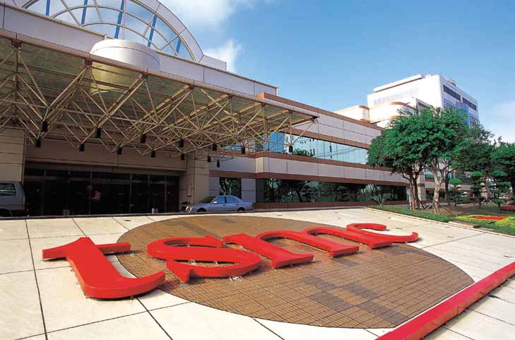
TSMC pioneered the pure-play foundry business model in 1987 and has been the world’s leading dedicated semiconductor foundry. The company supports a thriving ecosystem of global customers and partners with the industry’s leading process technologies and portfolio of design enablement solutions to unleash innovation for the global semiconductor industry.
With global operations spanning Asia, Europe, and North America, TSMC serves as a committed corporate citizen around the world.
TSMC deployed 281 distinct process technologies and manufactured 11,617 products for 510 customers in 2020 by providing broadest range of advanced, specialty and advanced packaging technology services.
TSMC is the first foundry to provide 5nm production capabilities, the most advanced semiconductor process technology available in the world.
SSS is a wholly owned subsidiary of Sony Group Corporation and leads in image sensors. Furthermore, the company’s semiconductor business also includes a variety of other parts, including micro displays, LSIs, and laser diodes.
- Share: