


ASIA ELECTRONICS INDUSTRYYOUR WINDOW TO SMART MANUFACTURING
Lam Research to Soar R&D with New US$3B Investments
Lam Research Corp. plans to invest more than US$3 billion over the next five years to expand its global research and development network, a move designed to accelerate semiconductor innovation and meet growing demand driven by artificial intelligence technologies.
The expansion will span multiple sites across Lam’s worldwide laboratory footprint and is expected to increase experiment capacity by more than 50%. The company said the initiative will strengthen infrastructure and technical capabilities across its integrated R&D ecosystem while helping customers speed new technologies from concept development to manufacturing deployment.
AI Demand Drives Need for Faster Development Cycles
As semiconductor manufacturers pursue more advanced chips for AI applications, the industry faces increasing complexity in device architectures, materials and production processes. Lam believes greater R&D velocity is becoming a critical competitive advantage.
“In the AI era, the pace of innovation is relentless, requiring chips with new architectures, different materials, and complex features engineered with nanoscale precision. Our ability to increase velocity throughout the R&D process has become a decisive advantage,” said Tim Archer, president and chief executive officer of Lam Research.
He added that the company is investing to stay ahead of customer requirements and strengthen its global innovation engine to support future semiconductor breakthroughs.
Global Lab Network Operates Around the Clock
Lam’s R&D network extends across the United States, Asia and Europe. The company combines specialized laboratories that focus on distinct stages of the innovation cycle with technology centers located near customer facilities.
Together, these sites function as an integrated 24/7 network that enables simultaneous innovation efforts across regions and time zones. The infrastructure currently supports more than one million experiments annually.
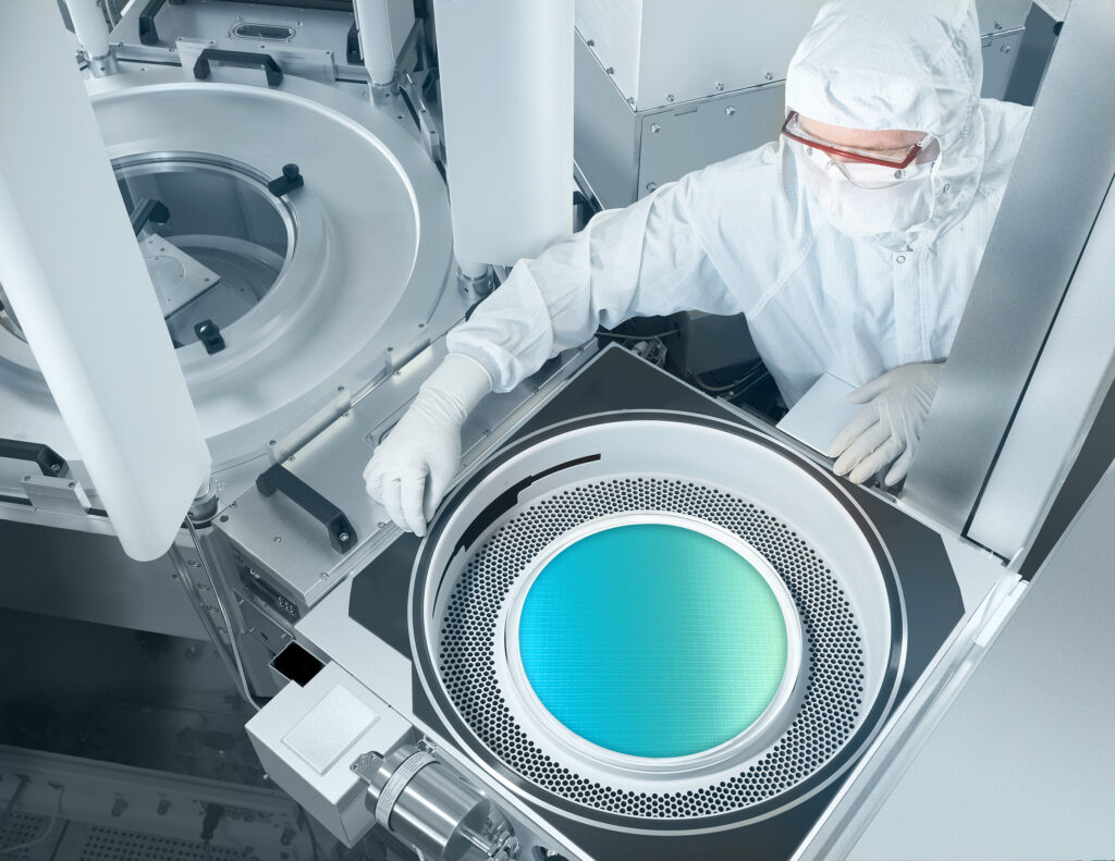
The company said its foundational research facilities focus on areas such as advanced chemistries, materials and mechatronics. In many cases, these labs can reduce experimental work that traditionally takes weeks to just a few days. Process development facilities then help move innovations toward production readiness by bringing engineering, product development and manufacturing teams together around the same tools and workflows.
Collaboration Model Speeds Customer Outcomes
A central feature of Lam’s strategy is close collaboration with customers. Technology centers located near customer operations support rapid qualification and validation activities, enabling engineering teams to work more closely on next-generation semiconductor technologies.
The company noted that its interconnected approach allows tools, data and expertise to be shared globally, ensuring discoveries made in one laboratory can quickly benefit other facilities. According to Lam, recent customer projects using this model shortened process development timelines by as much as 2.5 times.
Expansion Set to Begin This Year
Lam plans to start expanding the global laboratory network this year, with the objective of increasing innovation velocity and helping customers bring advanced semiconductor technologies into production more quickly.
As AI-related demand continues to drive investment across the semiconductor industry, the company is positioning its expanded R&D infrastructure to support faster innovation, technology scaling and manufacturing readiness.
17 August 2026
- Share: