ASIA ELECTRONICS INDUSTRYYOUR WINDOW TO SMART MANUFACTURING
Imec Establishes First Japan R&D Hub in Hokkaido
Imec is establishing its first research and development base in Japan, expanding its presence in Hokkaido as part of a broader effort to advance next-generation semiconductor and photonics technologies while strengthening collaboration across Japan’s growing chip ecosystem.
Backed by Japan’s Ministry of Economy, Trade and Industry (METI) and conducted in collaboration with the Leading-edge Semiconductor Technology Center (LSTC), the initiative moves imec beyond research partnerships and into a locally embedded R&D role. The organization plans to build a team of approximately 15 researchers and engineers in Hokkaido over the next five years, creating a permanent research presence connected to imec’s global operations in Belgium and elsewhere.
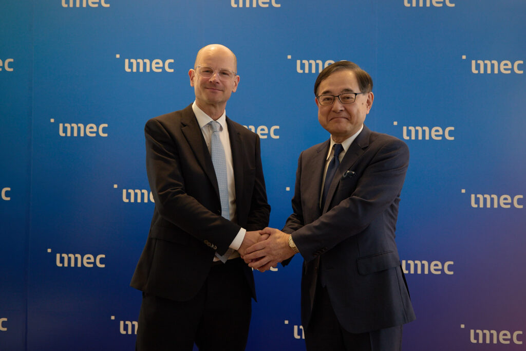
The strategic focus is on photonic integrated circuits (PICs), electronic-photonic integrated circuits (EICs), and co-packaged optics technologies, areas increasingly viewed as important for enabling more energy-efficient AI and high-performance computing systems.
Focus on Photonics and AI Infrastructure
According to Patrick Vandenameele, CEO of imec, the expansion is intended to strengthen the connection between Japanese innovation and the organization’s global research ecosystem.
“Japan plays a vital role in the global semiconductor ecosystem, with world-class expertise spanning materials, equipment, manufacturing and research,” said Patrick Vandenameele. “Through our R&D activities in Hokkaido, we aim to contribute to Japan’s ambitions in next-generation semiconductor and photonics technologies while further strengthening the connection between Japanese innovation and our global R&D ecosystem.”
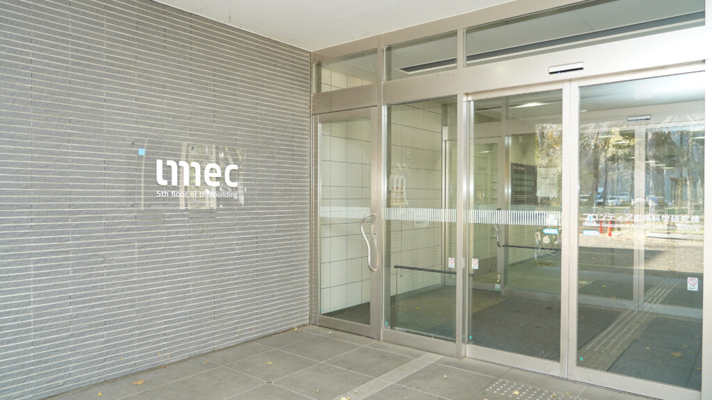
The Hokkaido team will collaborate with organizations including Hokkaido University, Tohoku University, Yokohama National University, AIST, and the Chitose Institute of Science and Technology to advance photonic and electronic-photonic integration technologies. The resulting innovations are expected to support future semiconductor platforms and commercialization activities involving industry partners, including Rapidus Corporation.
Builds on Earlier University Partnership
The new R&D center builds on a relationship established in November 2024, when imec and Hokkaido University signed a letter of intent to collaborate on semiconductor technology development, including work related to 2nm semiconductor use cases, joint research projects, specialized training, and PhD-level collaboration.
That relationship has since progressed into active initiatives, including co-packaged optics research in advanced semiconductor packaging and medical AI applications, as well as graduate student training programs.
“By bringing together leading universities, research institutes and industry partners, we can accelerate innovation on common ground and help create the technologies that will power future generations of AI and digital infrastructure,” Patrick Vandenameele said.
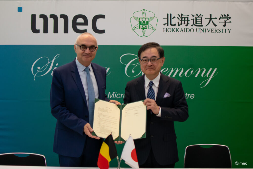
Kiyohiro Houkin, President of Hokkaido University, emphasized the importance of the new center in strengthening talent exchange and collaboration between Japan and Europe.
For semiconductor executives, equipment suppliers, packaging specialists, and investors, the announcement highlights the growing alignment between photonics research, advanced packaging development, and future AI computing requirements, while positioning Hokkaido as a more prominent location within Japan’s expanding semiconductor innovation network.
16 November 2026
- Share: