ASIA ELECTRONICS INDUSTRYYOUR WINDOW TO SMART MANUFACTURING
Panasonic Realizes Flow Soldering for 0603 Chips
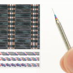
Miniaturization of chips is the main trend in electronic components. Recently, downsizing from 1608 to 1005 to 0603 sizes has been rapidly advancing (Fig. 1).
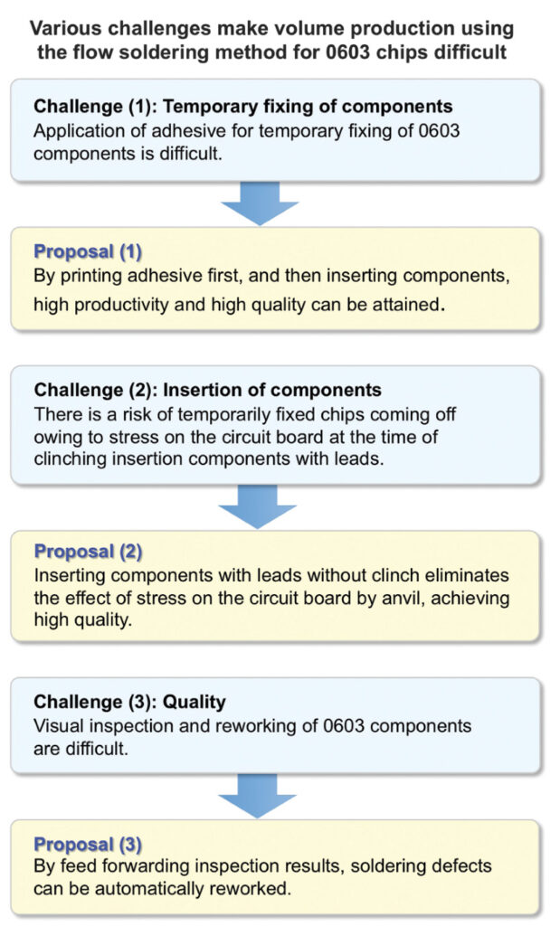
A growing number of manufacturers has been seeking the expertise of Panasonic Smart Factory Solutions Co., Ltd. (PSFS) in downsizing of chips to 1005 size. They also consult the company on process to support 0603 chips in terms of flow soldering method. Prior to the construction of flow soldering process to support volume production of 0603 chips, various challenges must be overcome (Fig. 2).
Challenges in Flow Soldering Process for 0603 Chips
In flow soldering of 0603 chips, the first challenge is the difficulty of adhesive application of φ0.3mm and smaller micro dot to temporarily fix 0603 chips. A dot of adhesive is applied by either dispensing method or printing method. The dispensing method enables the application of dots of up to about φ0.6mm. This means the 1608 size is the smallest component size that can be supported by this method. Meanwhile, thick masks are used for the printing of adhesive in the printing method. This process protects the leads of radial and axial components that have already been mounted on the circuit boards. This makes the aspect ratio large, causing difficulty in the printing of dots with microscale aperture diameter.
Second, shock and upward warpage of the printed circuits are at risk of occurring when clinching lead wires of components with leads. These components, which have been inserted into printed boards on an anvil, cause the chips temporarily fixed in the preceding process to come off.
Third, visual inspection of 0603 chips and repair of soldering defects are difficult.
Proposals to Solve Challenges
The first challenge can be solved by inserting components with leads after printing of adhesive. This enables the printing of adhesive using a thin mask, and hence application of micro dots of φ0.3mm and smaller that support 0603 chips.
Next, the second challenge can be solved by inserting all components with leads, including radial and axial components, into printed circuit boards without clinching. This enables high-quality mounting free from the coming off of temporarily fixed chips.
The third problem can be solved by adopting automatic
inspection, and feed forwarding the results to the point soldering equipment. This enables even automatic rework of soldering defects.
Board Manufacturing Process for 0603 Flow Process
A board manufacturing process that realizes the flow soldering process for 0603 chips is shown in Fig. 3 (This time, double-sided printed circuit boards using reflow and flow soldering are imagined). The process is broadly divided into three processes: 1) reflow mounting process → 2) process to temporarily fix chips onto the flow surface using adhesive → 3) process to complete circuit boards using flow soldering.
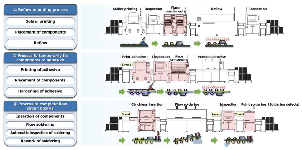
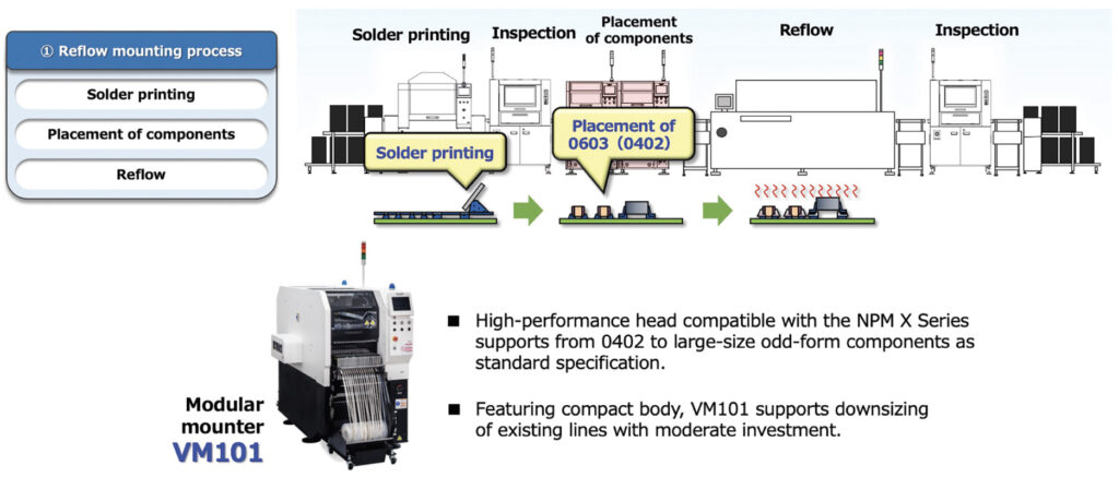
Reflow mounting process
Microchips and quad flat packages (QFPs) are mounted in the reflow process. As the downsizing trend of chips continues, the adoption of 0402 chips in addition to 0603 chips in the reflow mounting process can be considered. In this process, adding and connecting PSFS’s VM101 compact modular mounter to the existing line enables customers’ existing lines to support 0402 chips with ease with moderate investment (Fig. 4).
① Process to temporarily fix chips onto the flow surface using adhesive
In this process, the company’s SPV screen printer is used to print its ADE510D adhesive (Fig. 5).
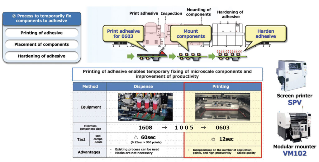
As the tact of the printing method does not depend on the number of application points, both high productivity and stable quality can be attained. ADE510D maintains stable viscosity even in the 24-hour continuous printing, and it features excellent shape retention property. As print shape does not change, it is effective for the printing of adhesive.
The position and quantity of the adhesive are inspected using an automated optical inspection system. Next, components are mounted using the company’s VM102 modular mounter, and then the adhesive is hardened in the adhesive hardening furnace to fix 0603 chips on the printed circuit board.
② Process to complete circuit boards using flow soldering
In this process, the company’s NPM-VF odd-form component insertion machine is used to insert components with leads (Fig. 6).
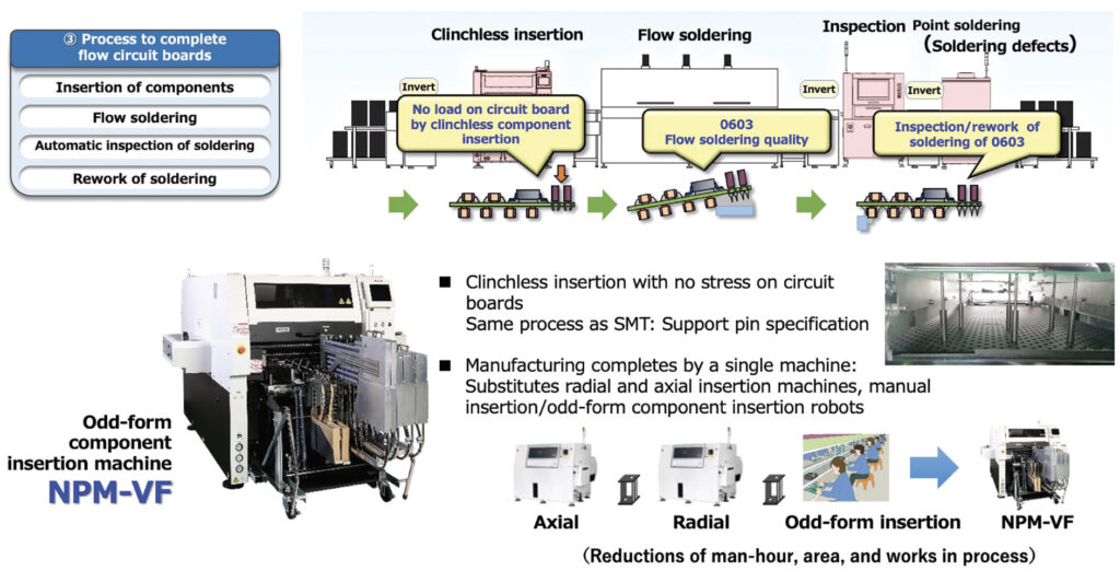
NPM-VF can insert radial and axial components into printed boards by cutting leads at the time of pickup. The support pin specification enables clinchless insertion. Hence, components are free from the shock and upward warpage stress that are applied to circuit boards at the time of clinching lead wires on an anvil. Thus, it is possible to minimize the risk of temporarily fixed chips coming off.
Meanwhile, NPM-VF can insert radial and axial components and odd-formed components using a single machine. Thus, it can achieve space savings, reduction of works in process, and reduction of man-hour for manual insertion.
Insertion components are flow soldered while attention is given to lifting of components, and automatic inspection of soldering conditions of all components from 0603 chips to components with leads is conducted. Then, based on the inspection results, automatic reworking of soldering defects is performed using a point soldering machine.
These processes realize the automation of visual inspection after soldering and unmanned reworking of soldering.
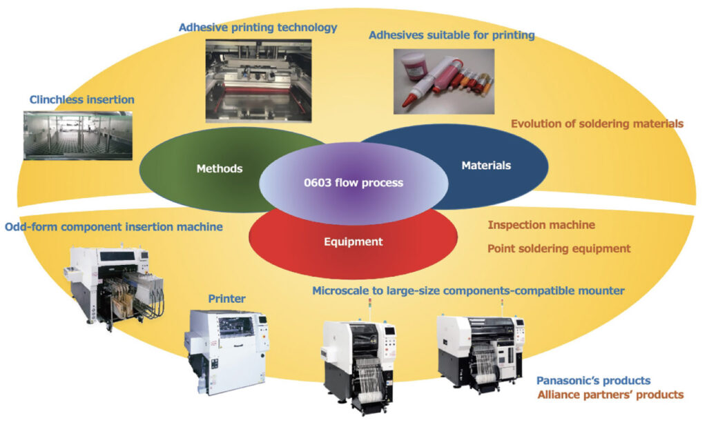
As described above, Panasonic contributes to the realization of the flow soldering process for 0603 components through coordination among machines, methods, and materials (Fig. 7).
- Share:


About This Article:
The author is Masahiro Sakata, Communication Promotion Department, Corporate Planning Department, Panasonic Smart Factory Solutions Co., Ltd. (PSFS).