ASIA ELECTRONICS INDUSTRYYOUR WINDOW TO SMART MANUFACTURING
Display Manufacturing Systems Parade at FINETECH Japan
The 31st FINETECH JAPAN LCD/OLED/SENSOR TECHNOLOGY EXPO was held From Dec. 8 to 10, 2021 at Makuhari Messe in Chiba Prefecture. The show highlighted the latest in display technologies and innovative applications.
This year’s event significantly diverted from the traditional show. Unlike the typical shows in the past, there were only few display manufacturers as exhibitors. The main exhibitors are materials, manufacturing equipment, and flat panel display (FPD) application manufacturers.
This article gives particular focus on Japan Science Engineering Co., Ltd.’s systems for trial production and manufacturing. It also includes a system for FPDs.
MX-1000 Series Maskless Exposure System
Structure, characteristics
The MX-1000 Series maskless exposure system employs Japan Science Engineering’s original Point Array high-speed imaging method. It is capable of directly drawing patterns. The MX-1000 Series provides direct imaging exposure for applications, such as research and development, trial production, and small-lot production. It can be used in the fine fabrication field, including micro electro mechanical systems (MEMS), as well as high-end printed circuit boards (PCBs), high-density packaging, and FPDs. Direct imaging exposure does not require photomasks in the lithography process, which minimizes development cost and time-to-market.
Fig. 1 shows the exterior view of the system and constituting technologies.
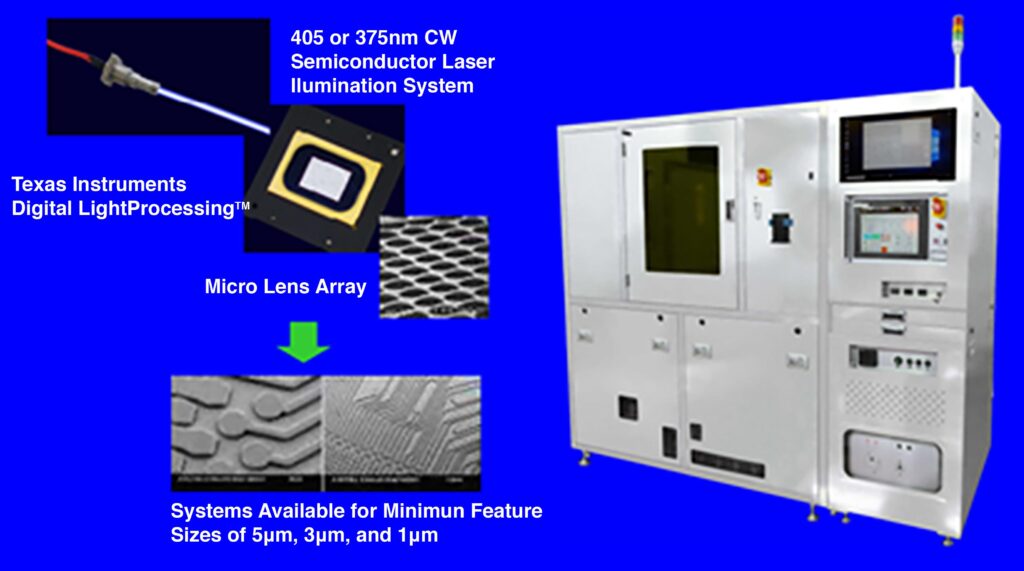
The MX-1000 Series maskless exposure system employs a 405nm or 375nm continuous wave (CW) semiconductor laser for the light source. It generates exposure patterns using Texas Instruments’ Digital Light Processing that uses digital micromirror device (DMD), eliminating the need for masks.
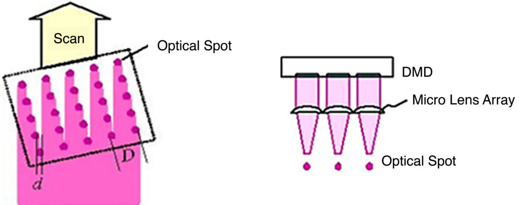
The Point Array method adopts a micro lens array to collect light from DMD’s each pixel (Fig. 2). It scans a group of optical spots that are obliquely arranged. With this, it achieves data resolution far smaller than the pixel size of the DMD without sacrificing the size of the lithography field. For example, when optical magnification is 5:1, it achieves data resolution of 0.05μm.
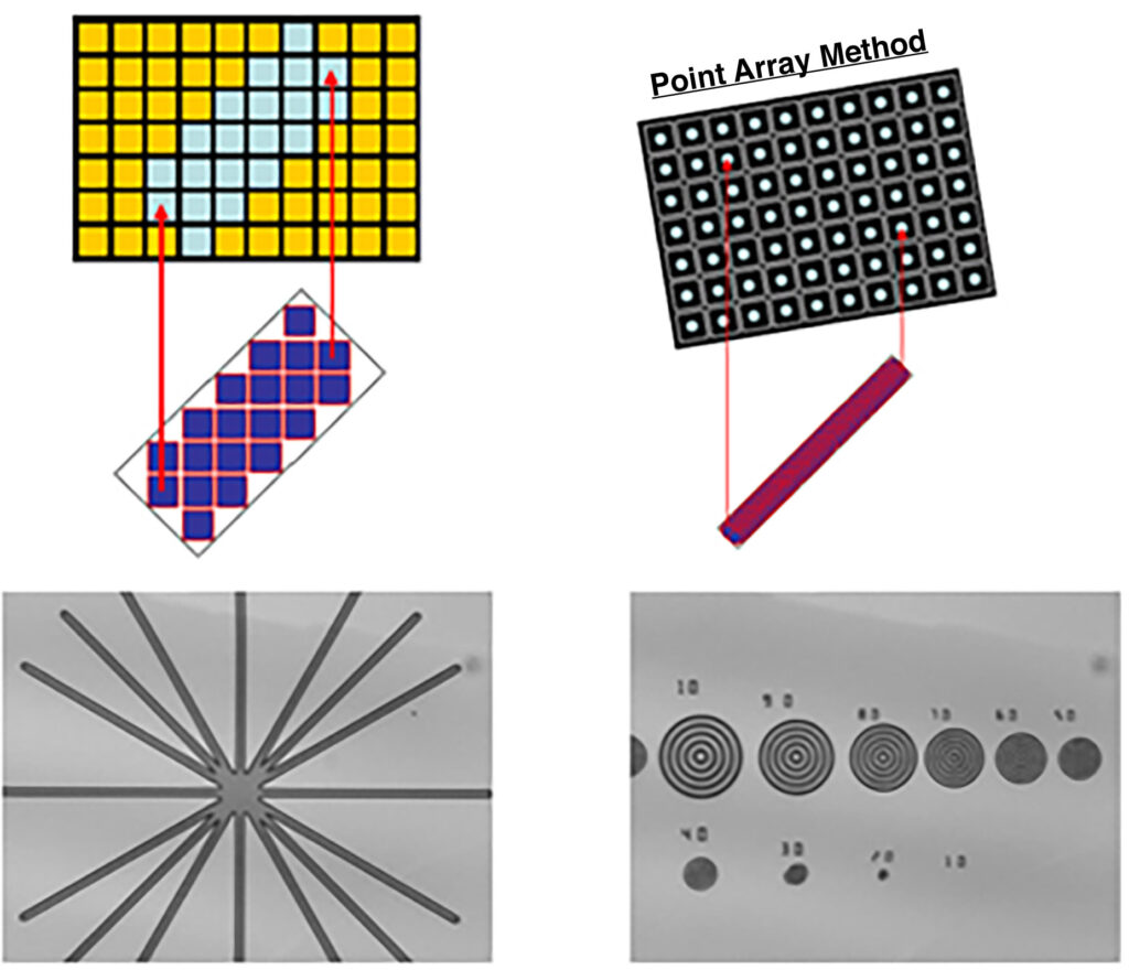
The Point Array method uses the collection of small points for exposure, making edges of oblique and curved lines smooth (Fig. 3).
Specifications, results of exposure
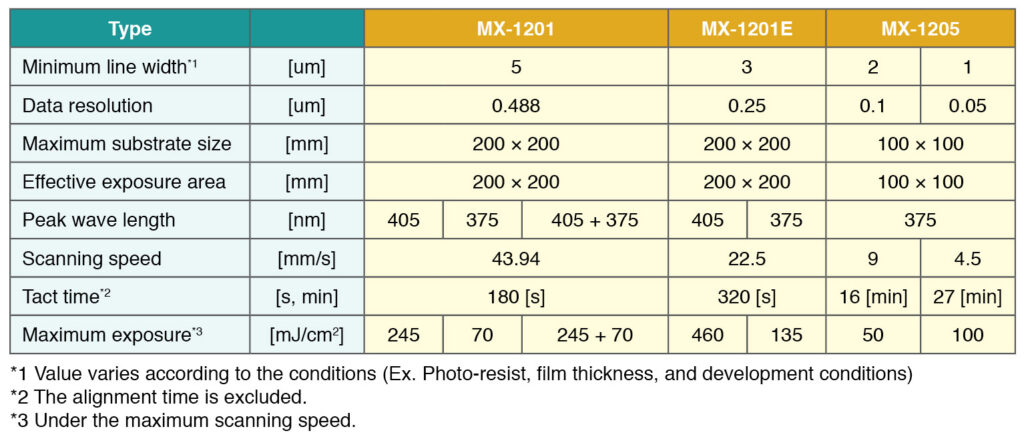
Table 1 shows the specifications of the MX-1000 Series maskless exposure system.
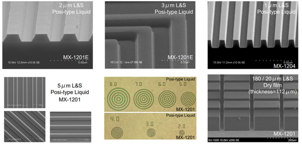
Meanwhile, Fig. 4 shows the results of exposure.
DA-1000 Desktop Mask Aligner
At the show, Japan Science Engineering also displayed the DA-1000 desktop mask aligner.
Photo 1 shows the exterior view of the DA-1000 exposure system designed for experiments and research and development.
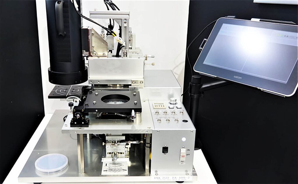
The DA-1000 mask aligner is optimal for experimentation and research applications. This manually operated system features a compact design (600×600mm) and can be mounted on a desk. It is equipped with an ultraviolet light-emitting diode (UVLED) lamp house as a standard specification with Ø4″ effective exposure range. The tool is a contact exposure type, while other exposure modes are available as an option.
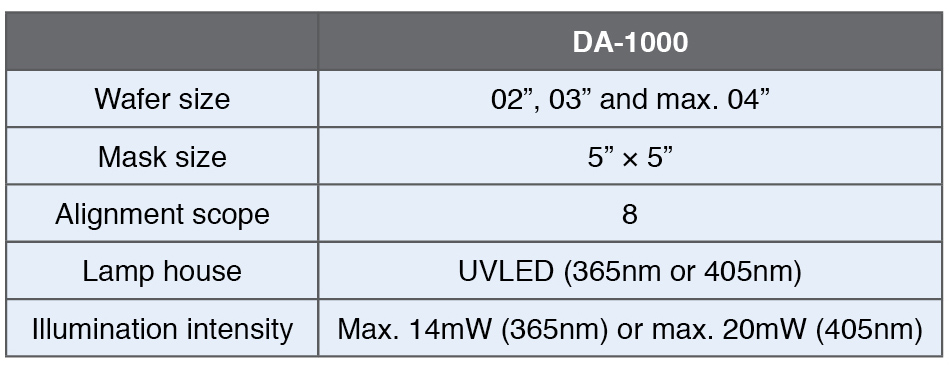
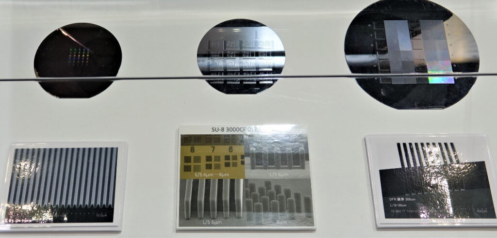
Table 2 shows the specifications of DA-1000, while Photo 2 shows samples of exposure patterns.
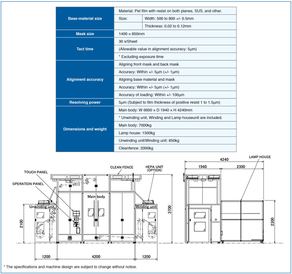
RA-6141B Roll-to-Roll Double-Sided Exposure System
The RA-6141B roll-to-roll double-sided exposure system supports film-like works, such as touch panels, electric paper, optical films, including three-dimensional (3D) films, and masks for organic light-emitting diodes (OLEDs). It also supports roll-to-roll processing and achieves mass production of flexible, thin and lightweight devices.
Photo 3 shows the exterior view of RA-6141B roll-to-roll double-sided exposure system.
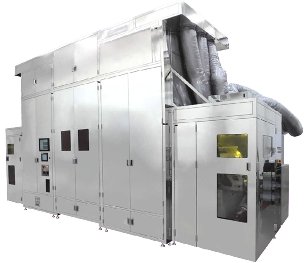
It employs vertical exposure with low tension on the base material. Auto alignment between a mask and base material enables multilayer exposure. It also supports mask cooling on an optional basis. It is designed for mass production of touch panels, flexible printed circuits (FPCs), OLED lighting panels, electronic paper, and solar cells.
Table 3 shows the specifications of the system.
About This Article:
The author, Yasuhiro Ukai, Ph.D., is from Ukai Display Device Institute (UDDI).
- Share: