ASIA ELECTRONICS INDUSTRYYOUR WINDOW TO SMART MANUFACTURING
New Method Meets Challenges in Micro-LED Production
The latest in display technologies took the spotlight at the recent 31st FINETECH JAPAN held at Makuhari Messe in Japan’s Chiba prefecture. The event also featured top-caliber technical seminars that focused on the latest breakthroughs in LCDs, OLEDs, and micro-LEDs for electronic display, internet of things (IoT), solid-state lighting, and other applications.
This article outlines one of the presentations in the event, which focused on micro-LEDs. The “Introduction of Total Solution for Micro LED Display Manufacturing” of Eiji Mori, Team Leader, Sales Dept., Sales Engineering Team, Mechatronics & Fine Technology Division, Business Div. I, Toray Engineering Co., Ltd. was one of the spotlight seminars. The author of this article has received permission for the printing of figures and tables.
Challenges in Manufacturing, Processes
Micro LED displays use minute LEDs measuring several tens of micrometers square. They do not require backlight, feature low power consumption, and long life. As such, they are attracting attention as environment-friendly displays. Furthermore, they also feature high contrast ratios, and high visibility of images. Thus, there has been much anticipation in the adoption of micro-LED displays in every device with a display, from smartphones, wearable devices to TVs.
Micro-LED displays require huge number of LED chips. For example, a 4K TV requires about 25 million chips (3,840×2,160 pixels each for three colors). It is indispensable to increase the transfer speed of micro-LEDs to achieve mass production of micro-LED displays.
Moreover, transfer technology using a laser has been developed, which has produced a certain result. Meanwhile, micro-LED chips, which are basically components, may include defects of 1 to 2 percent. A defect rate of 1 percent means there will be about 250,000 defective chips to manufacture a 4K TV. The conventional technology requires about 49 hours to repair them into quality chips. Thus, defective chips have been the bottleneck in mass production of displays.
Challenges in the manufacture of micro-LED displays and corresponding processes are 1) repair process: improvement of yield; 2) reduction of display unevenness (MURA); and 3) improvement of productivity.
Process Flow of Micro LED Displays
In the seminar, Mori introduced two mass transfer methods. They are 1) the Pick & Place method and the 2) Laser Transfer & Carrier Bonding method. This section introduces the outline of the Pick & Place mass transfer method. It also discusses the Laser Transfer & Carrier Bonding mass transfer method, announced recently in detail.
Mass Transfer ① : Pick & Place
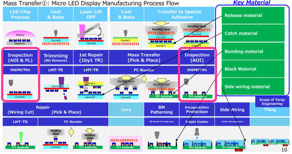
Fig. 1 shows manufacturing process flow of micro-LED displays ①. The processes consist of inspection, trimming, repair, mass transfer, and inspection. Main materials used in the processes are shown on the right side of the figure.
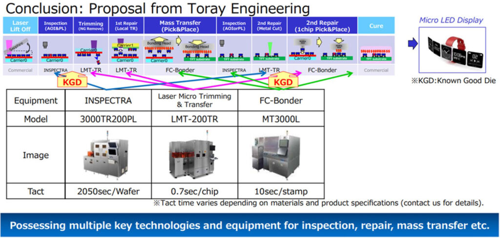
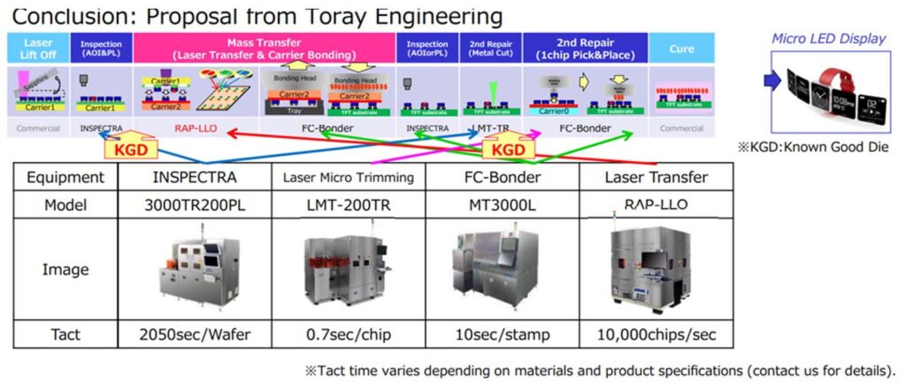
By way of conclusion, Fig. 2 shows the process flow and Toray Engineering’s production equipment used in each process and tact time of each equipment.
Mass Transfer ② : Laser Transfer & Carrier Bonding
Toray Engineering has developed the Random Access Patterned – Laser Lift Off (RAP-LLO) method. The RAP-LLO method’s distinct characteristics include 1) ability to select only good chips for transfer; 2) uniformity in emission luminance and emission wavelength through use of artificial intelligence (AI) software; 3) high-speed transfer (10,000 chips/sec); and 4) conversion of LED pitch into display pitch.
Fig. 3 shows manufacturing process flow of micro-LED displays ②.
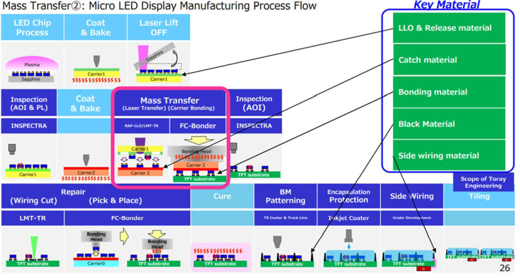
Fig. 4 shows the concept of high-speed laser transfer technology. RAP-LLO equipment plays role in the process to mount a large volume of micro-LEDs on a display substrate. The process whose efficiency enhancement has been warranted in the manufacturing process of micro-LED displays. It improves productivity to about 10-fold that of the conventional equipment.
RAP-LLO comes with Chip Mapping Algorithm, which Toray Engineering has originally developed applying AI technology. It also has a function to achieve displays with natural emission and colors. This was possible by judging the emission tendency of individual micro-LEDs and optimizing where in the display to arrange individual LEDs.
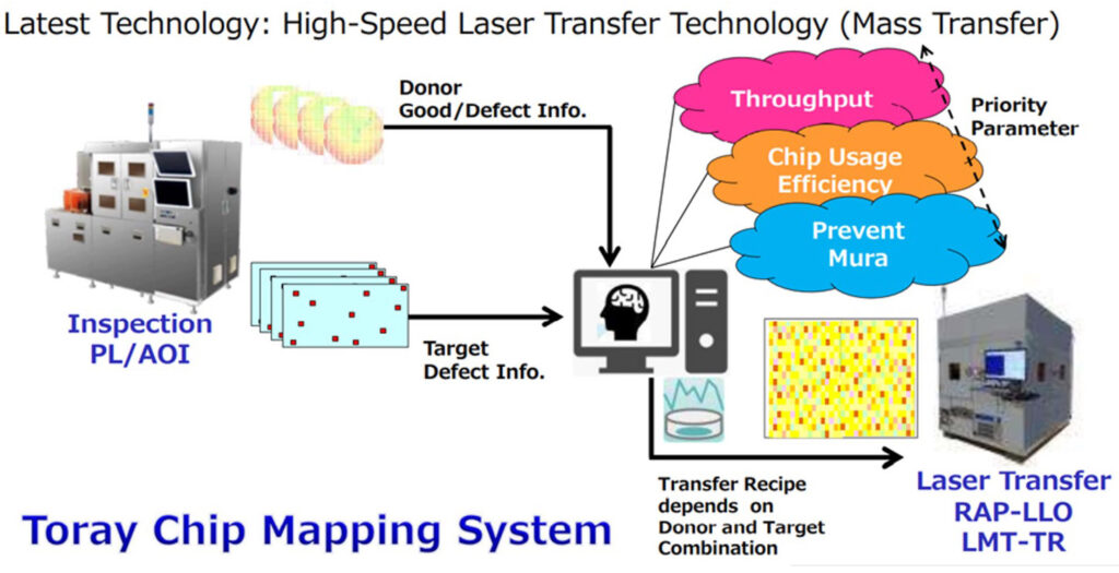
Fig. 5 shows challenges of existing manufacturing processes of micro-LED displays and the feature of the RAP-LLO high-speed laser transfer technology. Existing manufacturing processes of micro-LED displays have challenges. First, the mass transfer of 8 million LEDs by 30mm pitch stamping takes 6 to 7 hours to create a 55- to 65-inch 4K TV panel. This is not commercially viable.
Second, a competing manufacturer proposes high-speed laser transfer. It may seem like a solution, but only on the assumption that 100 percent good chips are on the LED panel. In fact, one can find 1 to 2 percent (80 to 160k) defective LEDs and transferred as they are.
In contrast, the RAP-LLO laser transfer equipment selects and transfers only good LEDs in high speed (13 to 22 minutes per panel). Hence, the technology is commercially viable.
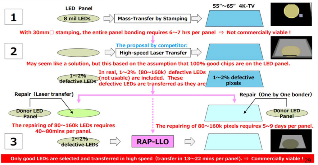
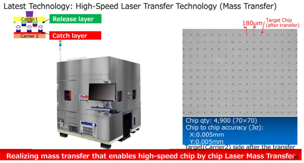
Fig. 6 shows the exterior view of the RAP-LLO equipment and the photograph of LED chips (70×70) after transfer.
By way of conclusion, Fig. 7 shows the process flow and production equipment ②.
Toray Engineering proposes the RAP-LLO to micro-LED display manufacturers targeting to receive ¥1 billion (approximately US$8.75 million) worth of orders in FY2022 and ¥5 billion (approximately US$43.73 million) worth of orders in FY2025.
- Share:


About This Article:
The author, Yasuhiro Ukai, Ph.D., is from Ukai Display Device Institute (UDDI).