ASIA ELECTRONICS INDUSTRYYOUR WINDOW TO SMART MANUFACTURING
Breakthrough Research Improves SiC Power ICs
Flexible 3D System Integration Laboratory (F3D) was established in Jan. 2020 as one of the official collaborative research institutes at Osaka University. Daicel Corporation, Senju Metal Industry Co., Ltd. (SMIC), and Yamato Scientific Co., Ltd. are the three core companies that made investments to the laboratory.
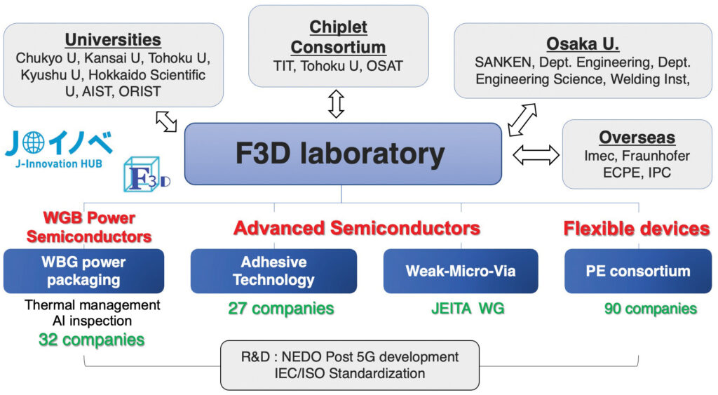
F3D Objectives, Activities
F3D is the 100th joint research course/collaborative research institute of Osaka University. It is directly under Osaka University and is based at the Institute of Scientific and Industrial Research (SANKEN), and is participated by Graduate School of Engineering, and Joining and Welding Research Institute. It is the first official organization under Osaka University to target open innovation.
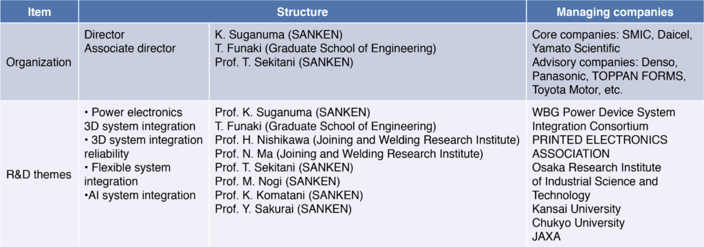
The objective of F3D is to deploy a platform to cultivate a new electronics area aimed at reliable manufacturing with the approval of the three core companies. Table 1 shows the structure and organization at its inception. Furthermore, adding the two existing study groups, F3D promotes activities shown in Fig. 1 as F3D System Integration Consortium.
The Ministry of Economy, Trade and Industry recognizes the F3D. It has also approved the said research institute as an open innovation house and selected as J-Innovation HUB in FY2020 (Fig. 1). Since its opening, F3D has carried out activities under difficult circumstances amid the COVID-19 pandemic.
Nonetheless, the webinars it started early on have attracted more than 100 people every time. Thus, they have been providing a forum for the dissemination of information on system integration of advanced semiconductors and next-generation power semiconductors toward the development of next-generation industrial technologies. Although there are many ways of promoting open innovation, F3D has received a strong response for its activities from the industry. Moving forward, it intends to seek best directions of the industry-academia partnership.
Next-Generation Power IC Packaging Technologies
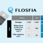
There is a growing demand for inverters for the control of power supplies of high-power motors for electric vehicles (HVs)/hybrid electric vehicles (HEVs), electric railway cars, and industrial robots. These scenarios are likely to increase the use of silicon carbide (SiC) semiconductors. SiC semiconductors withstand heat generation at power conversion between direct current (DC) and alternating current (AC) and feature small energy loss. To expand the SiC semiconductor market, needs for the development of joining technology and module structure that have excellent heat resistance and heat dissipation property have been increasing. A major challenge of power modules is how to achieve an ideal heat dissipation structure.
However, power modules that have thus far been put to practical use generate large thermal resistance as solders and grease are used. Specifically, thermal management is an indispensable technology not only for power semiconductors but also for advanced semiconductors that have been promoted as a national policy for artificial intelligence (AI)/internet of things (IoT) and post 5G. It is the target of global technological development race.
F3D has advanced the silver (Ag) micron-particle sinter joining technology over many years. It has already established Ag sinter joining technology with excellent performance without scarifying costs.[1] Recently, it has found that direct joining without plating is possible.[2,3] In conventional packaging technologies, in general, soldering is used for die attach, and grease is used for the connection to heat sink. However, these technologies have large thermal resistance and hamper heat dissipation, and hence, they have been hindering performance enhancement of power semiconductors.
Ag has a unique property to adsorb and desorb oxygen at temperatures around 200℃. In addition, it can also generate nanoparticles in large quantity, which is called “Ag nano-volcanic eruption.”[4] This phenomenon promotes sintering and joining. This mechanism enables direct joining of aluminum (Al) using Ag particles without plating.
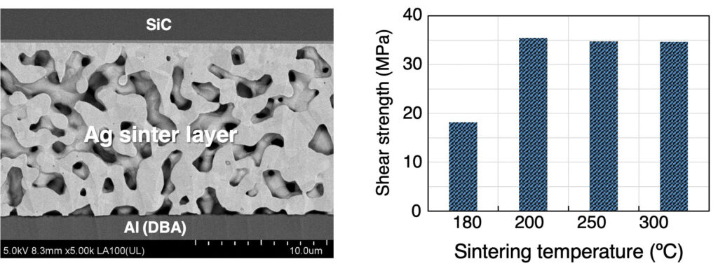
Fig. 2 shows an interface of pressure-less joining of SiC to direct bonded aluminum (DBA) (aluminum nitride (AlN) substrate) at 200℃ using Ag particle paste developed by F3D. Sintered Ag particles have a microporous structure.
In this state, Ag particles have joining strength (shearing) of 30Mpa or larger, and thermal conduction of 150W/mK, which are far larger than those of solder joining.
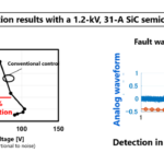
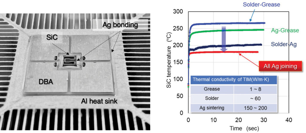
Fig. 3 shows an SiC die mounted on an Al heat sink making use of this property of Ag. In general, Al heat sinks have intricate shapes, such as a fin, and hence, pressure joining is not possible. Joining of a large area is also difficult. Certainly, it is not possible to directly join Al using solder, and hence, metalizing using nickel (Ni) or other metal is necessary. In addition, soldering forms a brittle intermetallic compounds (IMC) layer at the interface.
Furthermore, Ni plating lacks flexibility, and can become a cause of the reduction of reliability. Ag sinter joining solves these problems all at once. Looking at the cooling capacity of the new packaging structure, it has been found that it lowers the junction temperature nearly 100℃ comparing with conventional methods of using solder die attach and grease.
Future Prospects
The development of the low-pressure Ag sinter joining technology has enabled joining of large-area cooling plates with intricate shapes. In addition, it has also eliminated the need for the metalizing of Al materials, achieving an ideal heat dissipation structure. It has also significantly reduced costs in the manufacturing process.
The series of development has improved the performance of SiC power semiconductors, achieve superior reliability compared with conventional products. At the same time, it has enabled low-pressure process without using nano technology. Thus, realizing even cost reduction. These technologies are expected to accelerate the implementation of new-generation power modules in society. Furthermore, they are expected to be used not only for power electronics but also for advanced semiconductors as a new system integration technology.
Finally, this research has been conducted as part of “R&D on innovative heat dissipation and failure diagnosis technologies for achieving next-generation power semiconductors with higher quality and high reliability. Particularly, under the “Research and Development Program for Promoting Innovative Clean Energy Technologies Through International Collaboration” in FY2020 by Japan’s New Energy and Industrial Technology Development Organization (NEDO).
References
1K. Suganuma: System integration of SiC/GaN power semiconductors and reliability evaluation technologies, NIKKAN KOGYO SHIMBUN,LTD. (2014.12)
2D. Kim, C. Chen, S. Nagao, K. Suganuma, Mechanical characteristics and fracture behavior of GaN/DBA die-attached during thermal aging: pressure-less hybrid Ag sinter joint and Pb-5Sn solder joint, J. Mater. Sci. Mater. Electron., 31(2020), 587–598.
3C. Chen, K. Suganuma, Large-scale ceramic–metal joining by nano-grained Ag particles paste sintering in low-temperature pressure-less conditions, Scripta Mater., 195 (2021), 113747.
4S.-K. Lin, S. Nagao, E. Yokoi, C. Oh, H. Zhang, Y.-C. Liu, S.-G. Lin, K. Suganuma, Nano-volcanic eruption of silver, Sci. Rep., 6 (2016), 34769.
5J. Yeom, H. Zhang, C.-F. Li, K. Suganuma, Ag particles for sinter bonding: flakes or spheres?, J. Mater. Sci. Mater. Electron., 30(2019), 18080–18087.
- Share:


About This Article:
The author is Katsuaki Suganuma of Flexible 3D System Integration Laboratory, Osaka University.