ASIA ELECTRONICS INDUSTRYYOUR WINDOW TO SMART MANUFACTURING
Unique Material Poises for Next-Generation Power ICs
The industry draws its attention to a unique gallium oxide (GaO) featuring significantly higher dielectric breakdown strength than silicon carbide (SiC). Japanese firm FLOSFIA Inc. has developed this as a new material for next-generation power semiconductors.
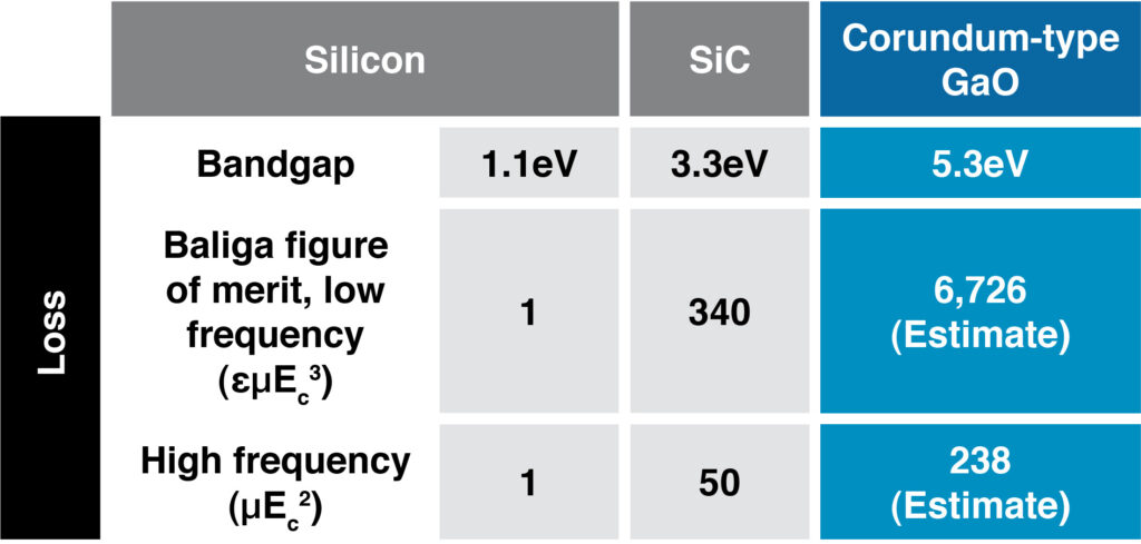
FLOSFIA handles corundum-type GaO (α-Ga₂O₃), which has a crystal structure of sapphire. It is characterized by a high bandgap of 5.3eV, which is about five-fold of silicon. It is also more than 60 percent larger than that of SiC (Table).
Generally, semiconductors with larger bandgap exhibit higher withstand voltage characteristics, or the strength to withstand voltage. A bandgap is an area wherein no electrons that carry electricity exist.
Semiconductors with larger bandgaps have smaller On resistance, or the difficulty of electricity flow in devices. Conditions required for power semiconductors are faster switching speed and larger power capacity. To satisfy these conditions, it is indispensable to improve withstand voltage and reduce On resistance. GaO attracts attention as a new material that meets these requirements.
Significant Dielectric Breakdown Strength
Corundum-type GaO can achieve thinness about 30-fold that of silicon and about quadruple that of SiC when they have the same withstanding voltage. Thus, corundum-type GaO can achieve smaller On resistance than existing materials.
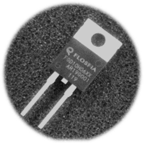
FLOSFIA plans to start mass production of Schottky Barrier Diodes (SBD) that employ corundum-type GaO by the end of the year. The company will adopt the TO-220 package, which is a general-purpose package, to encourage its widespread use.
Mist Dry Method
FLOSFIA’s strength is its proprietary crystal growth technology called the mist dry method. This method, which combines the wet method and the dry method, does not require a vacuum. As crystals can be grown at atmospheric pressure and at about 600℃, a burden on substrates due to temperature rise can be restrained in this method.
Material in mist form vaporizes before reaching the heated sapphire substrate, and crystal is grown through gas phase reaction. “The phenomenon may be pictured by imagining how a water droplet drops on a hot frying pan and bounces about,” explains Takuto Igawa, Vice President of Sales.
Retains Thermal Resistance
Conventionally, poor heat dissipation has been a weakness of GaO. However, FLOSFIA has overcome this problem by adopting a metal for support substrate. “The company has achieved thermal resistance on par with devices using other materials,” said Igawa. This was achieved by sandwiching about 10µm-thick GaO with metal layers.
To prevent the leakage of its core technology, the company adopts a semi-fabless business model for the manufacture of GaO power devices. Moreover, it has conducted design and epitaxy processes in-house.
However, amid the growing issue of the delay of semiconductor deliveries, the company has decided to conduct the front-end wafer process, or the separation of wafers into chips, at its own plant. Thus far, the company has outsourced the front-end process.
Igawa says, “The congestion of the front-end wafer process is a factor of the tight supply-demand balance of semiconductors.” Users have been highly evaluating the company’s decision from the viewpoint of business continuity.
Commitment to Sustainability
FLOSFIA advocates “semiconductor ecology,” aiming to reduce environmental load in the semiconductor manufacturing process.
Gallium is produced as a byproduct of aluminum production and has high recycling rate.
GaO power devices are also expected to reduce waste in terms of the process and power conversion efficiency in the manufacture of GaO semiconductors.
FLOSFIA intends to pitch GaO power devices to users who place importance to energy-saving feature in procuring materials.
- Share: