ASIA ELECTRONICS INDUSTRYYOUR WINDOW TO SMART MANUFACTURING
Intel Innovations Pave Way for Advanced Chip Packaging
Intel’s advanced packaging technologies extend and drive Moore’s Law as the company aspires to have a trillion transistors in a package by 2030. Moreover, Intel has led the industry in advanced packaging for a couple of decades. Its innovations include embedded multi-die interconnect bridge (EMIB) and Foveros. Most importantly, these technologies allow multiple chips on a package to be connected side by side (EMIB) or stacked on top of one another in a 3D fashion (Foveros).
“As Moore’s Law has been progressing, traditional scaling has been slowing down,” says Ann Kelleher, executive vice president and general manager of Intel’s Technology Development. “But as we start doing advanced packaging and heterogeneous integration, it means we can pack a lot more components into a given package and a given product.”

CHIPS Act Fuels R&D
Intel’s packaging technology is also a competitive advantage for Intel Foundry Services (IFS). Mark Gardner, senior director of Foundry Advanced Packaging with IFS, said the company, based on feedback he got from foundry customers, has been a trusted technology company with a proven track record. In addition, Gardner said, “Because we have such scale, we have a capacity and a geographic footprint that makes us much more diverse than some of the suppliers they work with today.”
With the passage of the CHIPS Act in the United States, Intel is doubling down on research and development (R&D) that will fuel new, leading-edge chip manufacturing facilities. Most importantly, these R&Ds will power today’s advanced technologies and tomorrow’s transformative innovations. Moreover, Intel is also investing in much-needed workforce development programs to ensure American workers have the necessary skills and talent to out-innovate the competition.
In 2021, Intel announced more than $43.5 billion in new manufacturing investments across Arizona, New Mexico, and Ohio to bolster U.S. chipmaking and R&D leadership. Since then, these investments have grown significantly, and they do not even account for our investments in domestic R&D or accelerated technology development.

Investments in Pipeline
The company has been expanding its operations in Arizona. For one, the location has been operating for more than 40 years. Most importantly, from the two factories when the facility started, it now has four leading-edge semiconductor factories estimated to cost US$15 to 20 billion each.
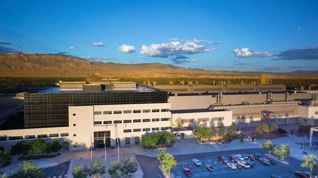
In New Mexico, Intel is investing at least US$3.5 billion in equipment upgrades for advanced semiconductor packaging operations. In fact, it is currently hiring to fill 200 of the 700 new manufacturing technician positions directly tied to this expansion.
Intel’s greenfield investment in two new leading-edge fabs in Ohio marks the single largest private-sector investment in the state’s history. This “Silicon Heartland” will establish a new regional economic cluster for U.S. chipmaking and become an epicenter of leading-edge technology.
In Oregon, Intel is in the planning phase for a multibillion-dollar expansion and modernization of our facilities that will put the company on a path to regain process technology leadership and continue to advance Moore’s Law.
In addition, Intel earlier announced a US$100 million investment to expand semiconductor education, research, and workforce training. This includes a US$50 million match for a total US$100 million partnership with the National Science Foundation to expand opportunities in the United States.
It also includes a US$50 million investment to fund the Intel Semiconductor Education and Research Program (SERP) for Ohio. Through this program, for example, Columbus State Community College has taken the lead in developing a one-year semiconductor technician certificate program that will launch in seven Ohio community colleges this fall term.


