ASIA ELECTRONICS INDUSTRYYOUR WINDOW TO SMART MANUFACTURING
Nepes Joins Hands with Siemens to Automate FO WLP Chip Packaging Process
3D chip-packaging maker Nepes of Korea and Siemens join hands to make chip packaging process more intelligent and more efficient
The Korean wafer-level chip packaging service provider said that it would introduce Siemens’ Xpedition HDAP or high density advance package tool to develop an automated chip packaging solution.
Siemens’s Xpedition HDAP tool is what is called as the industry’s first comprehensive solution for design and verification of leading-edge IC packaging designs.
Developed by Siemens’ Mentor business unit, it is an end-to-end solution to do rapid prototyping of heterogeneous substrate package assemblies.
The tool is an answer to challenges facing chip-packaging companies, as advanced chip packaging technologies like fan-out wafer level packaging (FOWLP) are rapidly emerging.
As chip packaging have to be done on a wafer substrate, calling for co-design of chip devices and packages, traditional HDAP flow becomes increasingly inefficient, taking days and weeks to prototype and verify chip-packaging processes.
Conversely, Xpedition HDAP flow can do protype evaluation and verification just in matter of just hours.
Working in sync with Xpedition HDAP, Nepes will automate a whole bunch of chip packaging processes from wafer-level package design to wafer mask creation to verification to documentation to wafer map array creation
“The cooperation work with Siemens will allow our customers to see and monitor all the chip packaging processes in one single integrated flow chart, ensuring reliability and efficiency.
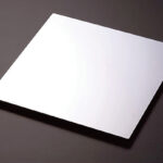
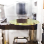
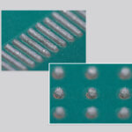
Called as fan-out wafer-level packaging or FO WLP, the new novel chip packaging technology is to pick and place chip dies to on a substrate called as a carrier and then mold them with proxy in what’s called as heterogeneous substrates or reconstituted wafer.
After the carrier is removed, IO or input and output pads are interconnected with solder bump in what’s called as redistribution layer, or RDL process to make contacts with other components.
The RDL is an extra bonding wires that can make chip-to-chip bonding or spread contact points or IO pads out of chip dies to make a connection with solder balls.
The invention of Fan-Out wafer-level packaging is to address the mismatch in the interconnection gap between real chip dies and PCBs, not only helping to secure more IOs, but also to reduce costs and time.
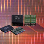
Nepes is one of the world’s largest Fan-out wafer-level package companies, serving big chip makers like Qualcomm.
The company is also working on a new breed of FO PLP, or fan out panel-level packaging technology.
- Share: