ASIA ELECTRONICS INDUSTRYYOUR WINDOW TO SMART MANUFACTURING
E&R to Propel Glass Substrate Use in New Alliance
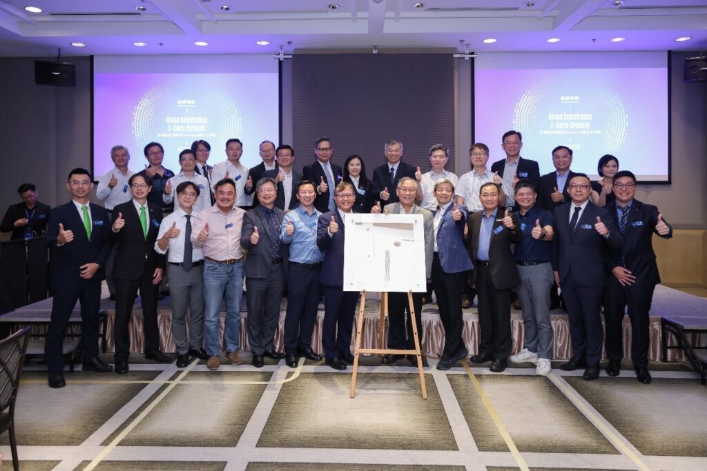
Taiwanese manufacturer, E&R Engineering Corp., launched the E-Core System, an initiative that led to the creation of the Glass Substrate Supplier E-Core System Alliance. Primarily, the alliance aims to combine expertise to promote comprehensive solutions, providing equipment and materials for next-generation advanced packaging with glass substrates to both domestic and international customers. E-Core System combines “E&R” and “Glass Core” and inspired by the sound of “Ecosystem.”
Specifically, E&R’s E-Core Alliance includes Manz AG and Scientech for wet etching; ShyaWei Optronics for automated optical inspection (AOI); Lincotec, STK Corp., Skytech, Group Up for sputtering and Ajinomoto Build-up Film (ABF) lamination equipment; and other key component suppliers, such as HIWIN, HIWIN Mikrosystem, Keyence Taiwan, Mirle Group, ACE PILLAR, CHD TECH, and Coherent.
Generally, E&R will continue leading the development of glass substrate technology in Taiwan. To this end, it will optimize processes and collaborate with more industry partners to achieve excellence.
Growing Importance of Glass Substrates
The rapid growth in demand for AI chips, high-frequency, and high-speed communication devices, increases the importance of glass substrates in advanced packaging technologies. Compared to the widespread use of copper foil substrates, glass substrates offer higher wiring density and better signal performance. Additionally, glass provides high flatness and can withstand high temperatures and voltages, making it an ideal replacement for traditional substrates.
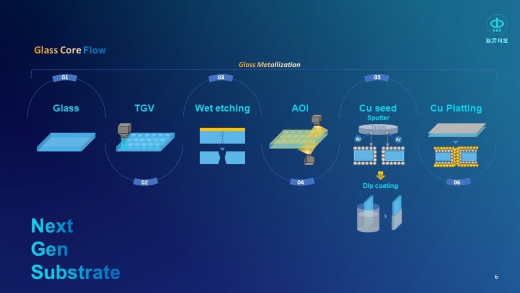
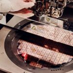
Primarily, the glass substrate process involves glass metallization, ABF lamination, and final substrate cutting. The key steps in glass metallization include Through-Glass Via (TGV), wet etching, AOI, sputtering, and plating. Specifically, these substrates measure 515×510mm, representing a new process in semiconductor and substrate manufacturing.
Glass Laser Modification TGV Technology
Mainly, the critical aspect of glass substrate technology is the first step—glass laser modification (TGV). Although introduced over a decade ago, its speed had not met mass production requirements. Specifically, it has achieved only 10 to 50 vias per second, limiting the market impact of glass substrates.
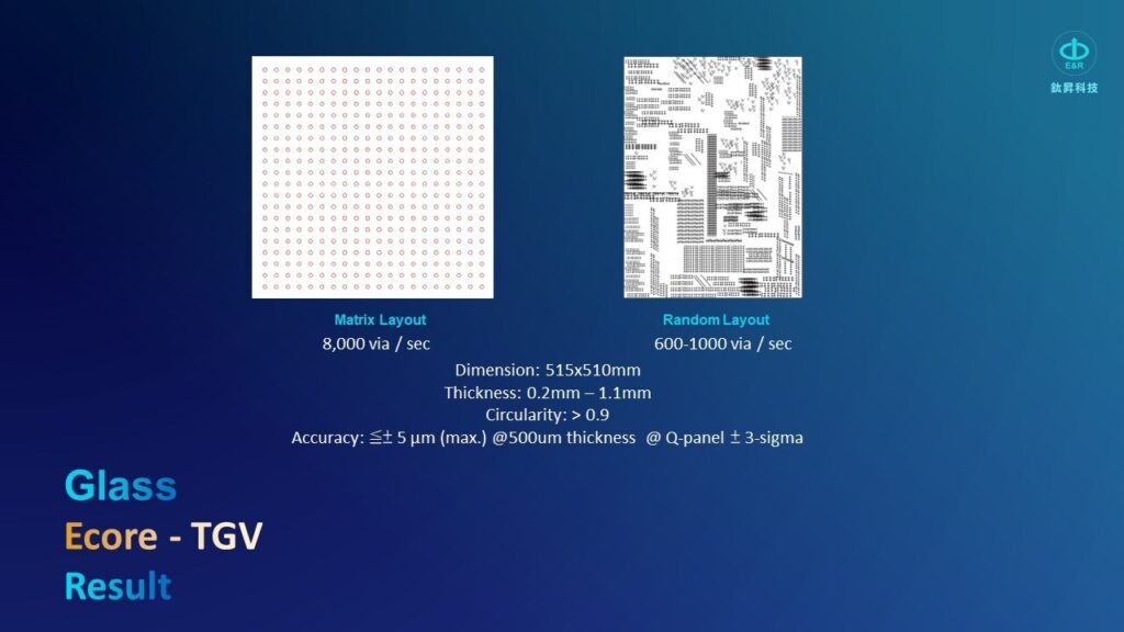
For the past five years, E&R Engineering has been working with a North American IDM customer to develop glass laser modification TGV technology. Last year, the process passed validation, with E&R mastering key technology, now achieving up to 8,000 vias per second for fixed patterns (matrix layout) or 600 to 1,000 vias per second for customized patterns (random layout), with an accuracy of ±5μm, meeting the 3 sigma standard. Accordingly, this breakthrough has finally enabled glass substrates to reach mass production.
E&R will also showcase the latest technologies at SEMICON Taiwan 2024 and SEMICON Europa 2024.
-02 September 2024-
- Share: