ASIA ELECTRONICS INDUSTRYYOUR WINDOW TO SMART MANUFACTURING
Reliable Device Test Improves Value of Components
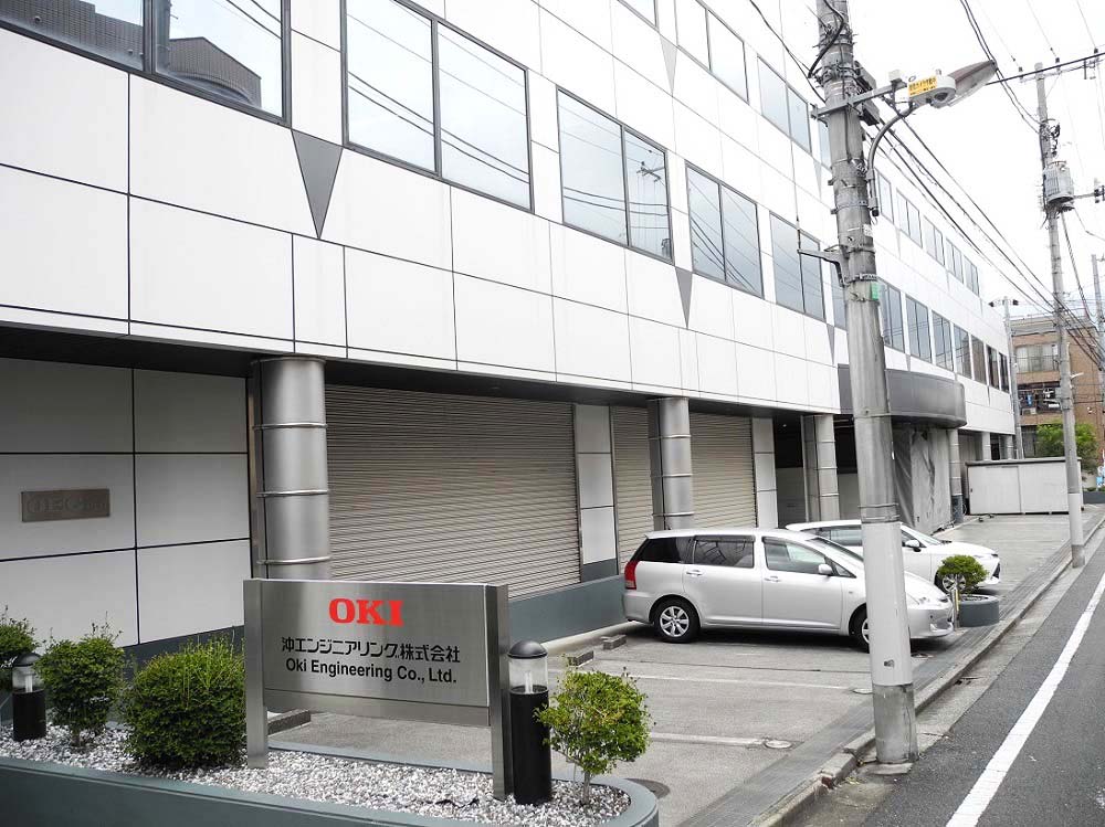
Oki Engineering Co., Ltd., a subsidiary of Oki Electric Industry Co., Ltd., tests semiconductors and electronic components and provide quality analyses structure, and screening. Its headquarters in Tokyo conducts evaluation analysis and device test as well as precision chemical and component analyses of devices.
In ruling out whether a device is a quality product or not, it is difficult to determine the cause of failure. The problem may have existed in the substrate or caused by connection failure. Therefore, analysis should start from the module.
Kei Takamori, General Manager of the Reliability Solution Division, Oki Engineering Co., Ltd., says, “We narrow down factors of problems to some extent by non-destructive inspections using infrared rays and X rays.” This is a procedure necessary to perform the subsequent destructive analysis with high precision.
Device Test to Specify Failed Portion
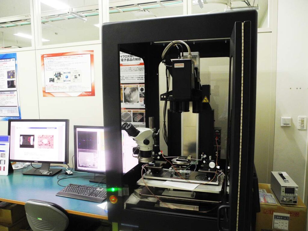
In the analysis room, an infrared camera helps detect heating of the mounted board and identifies failed portion. Applying voltage with a probe can detect heat due to short-circuiting and leakage current in defective products. This is because they have different current values from quality products.
Scraping the resin sealing of ceramic capacitors and other devices enables the specification of heat source more precisely. It is also possible to test devices by exposing the surface of chips.
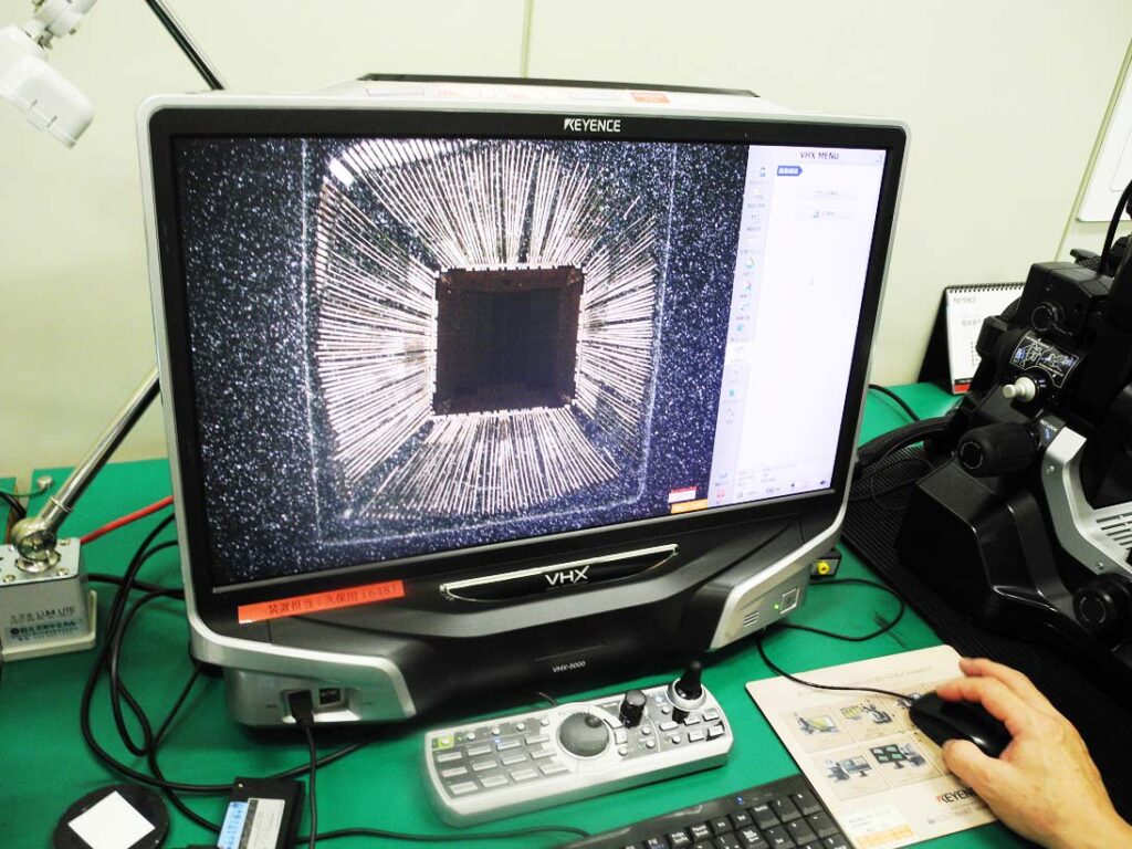
Once the test estimates the source of the failure, the use of X-ray transmission system, X-ray CT scanner or ultrasonic detection microscope will provide detailed analysis. Irradiating X-rays onto the sample enables non-destructive observation of the internal state of devices. From images shown on the display, one can deduce breakage of bonding wire or other causes of failure.
Lastly, the use of an optical microscope, with a magnifying power of about 2,000, will be useful in visual checking in the specified location of failure. The process will confirm the nature of the failure.
Evaluation of Electrical Characteristics
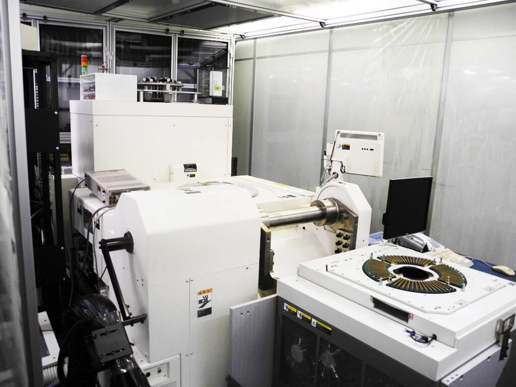
The tester room comes equipped with a range of equipment for performing electric characteristics evaluation of LSIs and analog devices. The LSI tester and wafer prober installed in the clean booth that secures cleanliness evaluate chips in wafer state before packaging. These instruments measure power consumption, input/output voltages, and operation frequencies of LSI chips formed on the wafer.
A semiconductor curve tracer also comes basic in a tester room. This evaluates electrical characteristics of power metal-oxide semiconductor field-effect transistors (MOSFETs) that are voltage control devices.
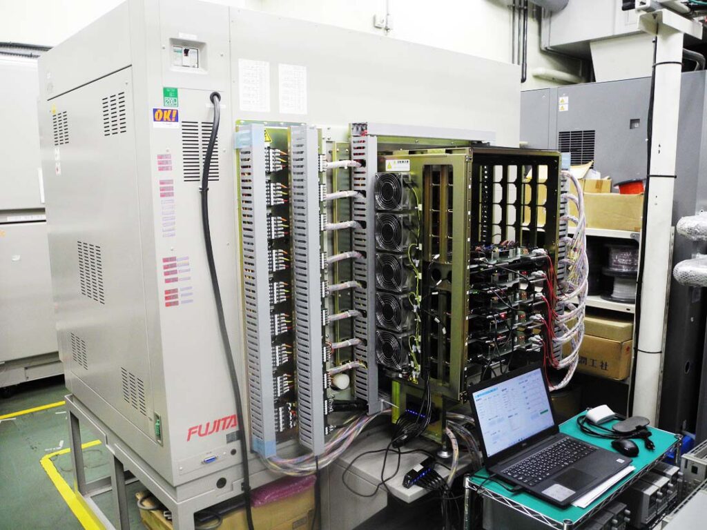
Oki Engineering started in March services analyzing burn out accidents of lithium-ion rechargeable batteries. The company determines causes of the ignition of the charging cell of electric vehicles (EVs) resulting from overcharging, and other cases. The company is receiving a dozen inquiries every month. In June, the company started services to determine authenticity of semiconductors. It is receiving a rush of orders amid the supply shortage of semiconductors in the market.
Oki Engineering handles evaluation tests of diverse objects. In particular, the company receives orders for various automotive-related tests. Its center in Honjo in Japan’s Saitama Prefecture has various types of large-scale equipment, including 10m anechoic chamber that conforms to international standards. It performs various tests assuming operation environments of automotive components, such as temperatures, shocks, and dusts, as well as electromagnetic compatibility (EMC) standard test.
