ASIA ELECTRONICS INDUSTRYYOUR WINDOW TO SMART MANUFACTURING
SK hynix Brings New 12-Layer HBM3E to Mass Production
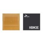
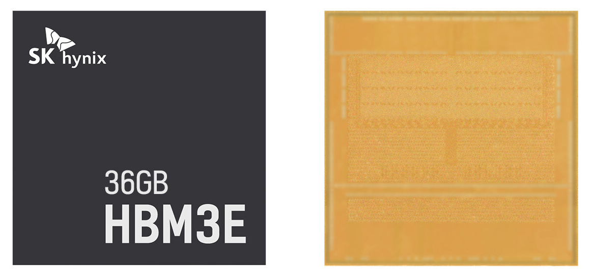
SK hynix Inc. has begun mass production of the first 12-layer HBM3E product with 36GB[1], the largest capacity of existing High Bandwidth Memory (HBM[2]) to date.
Accordingly, the company plans to supply mass-produced products to customers within the year, proving its overwhelming technology once again six months after delivering the HBM3E 8-layer product to customers for the first time in the industry in March this year.
SK hynix is the only company that has developed and supplied the entire HBM lineup from the first generation (HBM1) to the fifth generation (HBM3E), since releasing the world’s first HBM in 2013. Further, the company plans to continue its leadership in the AI memory market, addressing the growing needs of AI companies by being the first in the industry to mass-produce the 12-layer HBM3E.
According to the company, the 12-layer HBM3E product meets the highest standards in all areas that are essential for AI memory, including speed, capacity and stability. Mainly, SK hynix has increased the speed of memory operations to 9.6Gbps, the highest memory speed available today. If ‘Llama 3 70B’[3], a Large Language Model (LLM), is driven by a single GPU equipped with four HBM3E products, it can read 70 billion total parameters 35 times within a second.
Particularly, SK hynix has increased the capacity by 50% by stacking 12 layers of 3GB DRAM chips at the same thickness as the previous eight-layer product. To achieve this, the company made each DRAM chip 40% thinner than before and stacked vertically using TSV[4] technology.
Moreover, the company also solved structural issues that arise from stacking thinner chips higher by applying its core technology, the Advanced MR-MUF[5] process. Specifically, this allows to provide 10% higher heat dissipation performance compared to the previous generation. Also, it secures the stability and reliability of the product through enhanced warpage controlling.
“SK hynix has once again broken through technological limits demonstrating our industry leadership in AI memory,” said Justin Kim, President (Head of AI Infra) at SK hynix. “We will continue our position as the No.1 global AI memory provider as we steadily prepare next-generation memory products to overcome the challenges of the AI era.”
[1] Previously, the maximum capacity of HBM3E was 24GB from eight vertically stacked 3GB DRAM chips.
[2] HBM (High Bandwidth Memory): This high-value, high-performance memory vertically interconnects multiple DRAM chips and dramatically increases data processing speed in comparison to traditional DRAM products. HBM3E is the extended version of HBM3, the fourth-generation product that succeeds the previous generations of HBM, HBM2 and HBM2E.
[3] Llama 3: Open-source LLM released by Meta in April 2024, with 3 sizes in total: 8B (Billion), 70B, and 400B.
[4] TSV (Through Silicon Via): This advanced packaging technology links upper and lower chips with an electrode that vertically passes through thousands of fine holes on DRAM chips.
[5] MR-MUF (Mass Reflow Molded Underfill): The process of stacking semiconductor chips, injecting liquid protective materials between them to protect the circuit between chips, and hardening them. The process has proved to be more efficient and effective for heat dissipation, compared with the method of laying film-type materials for each chip stack. SK hynix’s advanced MR-MUF technology is critical to securing a stable HBM mass production as it provides good warpage control and reduces the pressure on the chips being stacked.
-27 September 2024-
- Share: