ASIA ELECTRONICS INDUSTRYYOUR WINDOW TO SMART MANUFACTURING
DNP to Surge Photomask Pitch for More Innovative ICs
Semiconductor manufacturing involves complex process and semiconductor equipment play crucial roles.
A semiconductor process has two major processes. First, the front-end process enables the film to form on the surface of a wafer made of silicon or other raw material and a circuit is drawn on it. Second, the back-end process in which the wafer is cut into chips, electrodes are formed, and packaging is performed to form the semiconductor device.
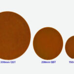
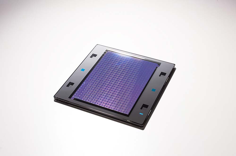
The most important part of the front-end process is the exposure process, which writes the circuit onto the wafer. In the exposure process, an exposure device is used to draw circuits by irradiating light onto the wafer through an original plate and lens called a “photomask,” which is used to transfer the circuit pattern. The narrower the line width of this circuit, the faster the data processing speed, which determines the performance of semiconductor devices. Currently, 3nm products are in mass production for cutting-edge devices, and development for further miniaturization is underway.
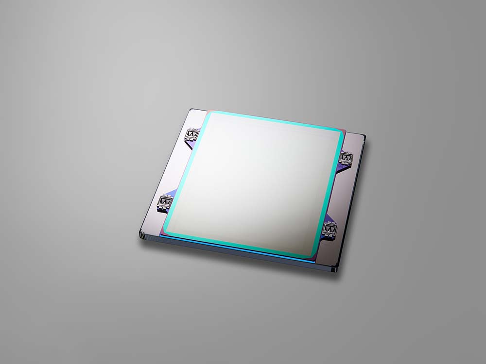
To form circuits with such ultra-fine line widths, exposure systems are also evolving. The most advanced semiconductor devices use EUV lithography equipment that uses extreme ultraviolet (EUV) light with a wavelength of 13.5nm. An essential part of the exposure process using EUV lithography equipment is the EUV photomask, which is the original plate for the circuit pattern. It requires a high level of technology that can realize finer and more complex pattern structures than the optical photomasks used in the conventional exposure process.
Makes Great Strides as Photomask Manufacturer
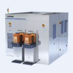
Dai Nippon Printing Co., Ltd. (DNP) designs, manufactures, and sells photomasks based on printing technology cultivated over many years. The company offers a lineup of photomasks not only for legacy semiconductors of 28nm or larger, but also EUV photomasks. Thus, contributing to the manufacture of cutting-edge devices. The company is focusing on these products as key products in the semiconductor-related business, one of its key business areas.
The photomask market comes into the “in-house production market” for semiconductor manufacturers and the “external sales market” for semiconductor manufacturers that do not have in-house production divisions. DNP targets the external sales market. Since the 2000s, competition for miniaturization has intensified, and major semiconductor manufacturers and foundries have accelerated their in-house production of photomasks for use in advanced processes. Although there was a time when DNP shifted its main focus from photomasks for advanced processes to those for legacy processes, the company continued to develop photomasks for cutting-edge processes.
Rapidus Provides Impetus
Established in 2010, Rapidus Corporation has been recently manufacturing cutting-edge semiconductor devices in Japan. From there, DNP changed course and began to focus on the photomask business in all directions, including photomasks for cutting-edge devices.
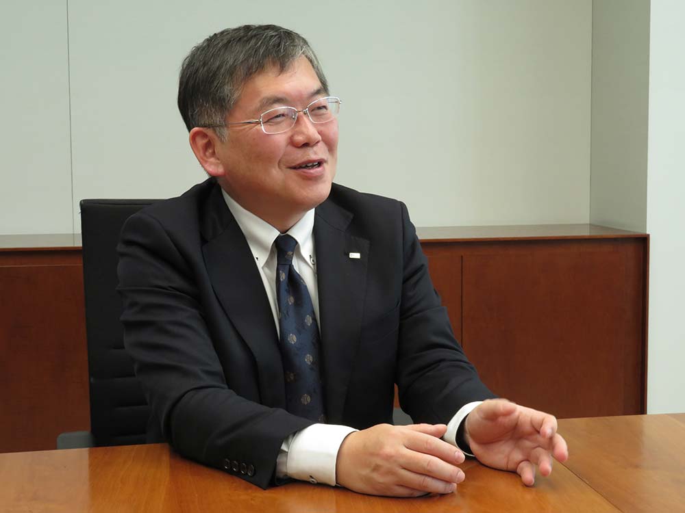
Minoru Nakanishi, Corporate Officer in charge of the photomask business, said, “The establishment of Rapidus was the signal for us to renew our efforts in all directions. Over time, semiconductor manufacturers have increasingly been allocating resources to research and development of cutting-edge devices, and some have begun to procure photomasks for non-advanced fields from external suppliers, whereas they used to manufacture their own photomasks in-house. DNP will focus on EUV photomasks and other cutting-edge products and expand its business by offering proposals to the in-house production market in addition to the external sales market.”
In March 2012, DNP participated as a subcontractor in the New Energy and Industrial Technology Development Organization (NEDO)’s “Post-5G Information and Communication System Infrastructure Enhancement R&D Project,” in which Rapidus is participating. We have been working on the development of a 2nm generation EUV photomask manufacturing process. In December 2012, they succeeded in resolving the fine patterns required for logic semiconductor photomasks of the 2nm generation and beyond. The company is steadily advancing development toward the realization of state-of-the-art device manufacturing using the 2-nanometer process.
Focuses on Nanoimprinting, Too
In addition to photomasks, the company is also working on the development of nanoimprinting. Nanoimprinting is a technology for forming circuits by pressing a plate (template) with a fine concavo-convex pattern onto a resin coated on a substrate. The company manufactures templates.
Although nanoimprinting has the advantage of reducing power consumption to one-tenth that of conventional exposure technology, there are some issues. Among them are particle contamination, because of the direct contact between the wafer and the template. DNP has been working on joint development with Canon and other companies since 2009, and in 2011 Canon developed and began selling nanoimprint equipment.
DNP expects that the needs for nanoimprinting will arise from companies seeking a different approach from the EUV process, which requires huge investment funds, and will make a proposal. Nakanishi said, “I think there are areas between the conventional optical mask area and the EUV mask area that can be replaced by nanoimprinting. We have already started to propose nanoimprinting, and inquiries have begun to come in. We will accelerate proposals together with the photomask business to expand our business.
Reinforcement of Volume Zone Business
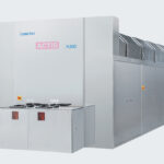
In addition to efforts in cutting-edge areas centered on EUV photomasks, the company will also strengthen its response to the volume-zone market. The company plans to invest 20 billion yen between FY2011 and FY2013. By renewing aging facilities, the production capacity for the volume zone in 2013 is expected to increase by 20% from the 2010 level. For cutting-edge areas, the company will invest in the expansion of multi-beam lithography systems, EUV mask inspection systems, and other equipment.
Nakanishi, Corporate Officer, said, “The semiconductor market will continue to grow steadily. We are aiming for growth that exceeds the growth rate of the semiconductor market. We will expand our business performance in both cutting-edge areas such as EUV and volume zones, which will lead to further growth. As competition with overseas companies intensifies, we will make the most of our strength, which is our ability to make proposals in all directions, to tackle this challenge. We will focus on providing value-added proposals so that our customers can trust us with their photomask-related problems,” he said.
This is an English translation of a Japanese article published in Dempa Shimbun Daily.
04 February 2024
- Share: