ASIA ELECTRONICS INDUSTRYYOUR WINDOW TO SMART MANUFACTURING
Latest DNP Photomask Process Suits 3nm EUV Lithography
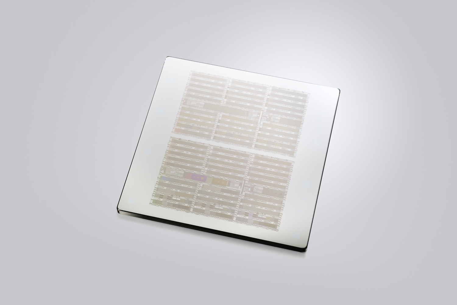
Dai Nippon Printing Co., Ltd. (DNP) has developed a breakthrough in photomask manufacturing process. Specifically, the latest process is capable of accommodating the 3-nm (10-9m) lithography process that supports Extreme Ultra-Violet (EUV) lithography, the cutting-edge process for semiconductor manufacturing.
Background
Over the years, DNP has continually responded to the demands of semiconductor manufacturers in terms of performance and quality. In 2016, it became the first merchant photomask manufacturer to introduce the multi-beam mask writing tool (MBMW). In 2020, DNP developed a photomask manufacturing process for 5nm EUV lithography processes. Since then, it has been supplying masks that meet the needs of the semiconductor market. In this latest development, the company has developed a photomask for EUV lithography capable of supporting 3nm processes. This aims to meet the needs for further miniaturization.
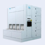
Specifically, the MBMW introduced by DNP in 2016 is capable of irradiating with approximately 260,000 electron beams. It can significantly shorten the lithography time even with complex pattern shapes. On this occasion, DNP has improved the manufacturing process by leveraging the characteristics of the equipment. At the same time, it optimized the data correction technology and processing conditions to match the complex curved pattern structure of the photomask for EUV lithography.
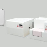
Today, DNP has installed a new MBMW, and plans to commence operations in the second half of 2024. The company will also strengthen its support for semiconductor manufacturing in advanced areas such as photomasks for EUV lithography.
DNP will promote the joint development of EUV photomasks for next-generation EUV exposure equipment with Interuniversity Microelectronics Center (imec), a leading international research organization headquartered in Belgium.
Going Forward
DNP will provide the newly developed photomask to semiconductor-related manufacturers throughout the world. In addition, it will also support the development of peripheral technologies for EUV lithography, targeting annual sales of 10 billion yen in 2030.
Through joint development with partners, such as imec, DNP will continue to develop more advanced photomasks capable of supporting processes finer than 3nm and even beyond 2nm.
- Share: