ASIA ELECTRONICS INDUSTRYYOUR WINDOW TO SMART MANUFACTURING
STMicroelectronics to Surge Chip Fab With New PLP Line
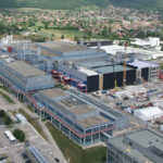
STMicroelectronics has announced investing about US$60 million to boost its pilot line in Tours, France for next-generation panel-level packaging (PLP) technology. Accordingly, the pilot line, which will become operational in Q3 of 2026, will expand the PLP capabilities of ST, one of the world’s largest chipmakers.
“The development of our PLP capabilities in our Tours site is aimed at advancing this innovative approach to chip packaging and test manufacturing technology, boosting efficiency and flexibility so it can be rolled out across a wide portfolio of applications, including RF, analog, power and microcontrollers,” said Fabio Gualandris, President Quality, Manufacturing and Technology of STMicroelectronics.

Enables Higher Manufacturing Throughput
The capital investment of over US$60 million, already allocated as part of the company-wide program to reshape the Company’s manufacturing footprint. Additional synergies are expected with the local R&D ecosystem, including the CERTEM R&D center. The program is focused on advanced manufacturing infrastructure and brings redefined missions for some sites in France and Italy to support their long-term success.
“With our fab in Malta, ST has already demonstrated its capability to deliver high-performing chip packaging and test in Europe. As we reshape our global manufacturing footprint, this new initiative in Tours will expand our process, design and manufacturing innovation capabilities supporting the development of next-generation chips in Europe,” said Gualandris.
PLP is an advanced, automated chip packaging and test process technology bringing increased manufacturing efficiency and reducing costs, and a key enabler for creating the next generation of smaller, more powerful, and cost-effective electronic devices.
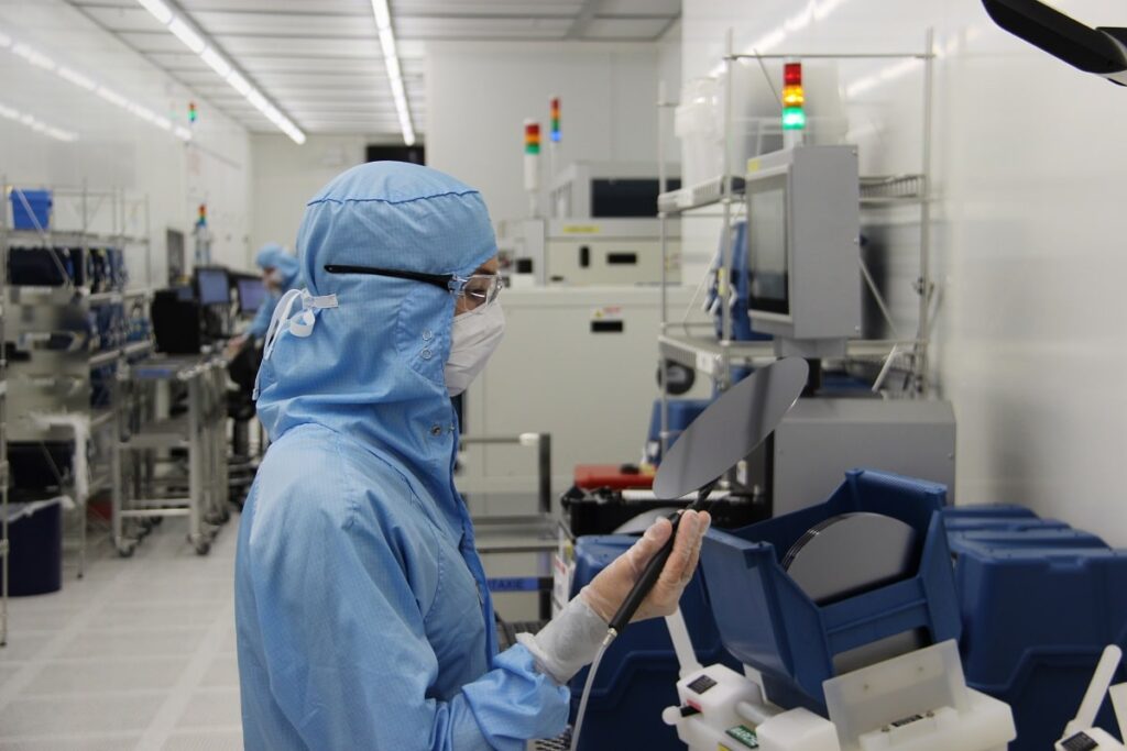
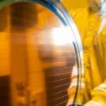
The PLP technology is a large rectangular-shape panels in place of circular wafers. It enables higher manufacturing throughput, making it a more efficient solution for high-volume production. The Tours pilot line builds on its first-generation PLP line in operation in Malaysia and its global technology R&D network.
PLP as Emerging Advanced Chip Packaging
For many decades now, the industry has relied heavily on wafer-level packaging (WLP) and flip-chip technology to connect silicon chips to external circuitry. However, as devices become smaller and more complex, the conventional methods are closely reaching their technical limits. PLP is one of the emerging approaches for advanced chip packaging.
Panel Level Packaging is a method where multiple ICs are packaged on a single, larger rectangular substrate panel, rather than on individual circular wafers. This allows for more ICs to be processed simultaneously, reducing costs and improving throughput.
ST’s PLP technology focuses on Direct Copper Interconnect (DCI). Direct copper interconnections replace the traditional wire connections of chips with their encapsulation support. DCI is the process by which these ICs are electrically connected to the panel substrate using copper, which is known for its excellent electrical conductivity.
ST has not only adopted PLP-DCI but has also been at the forefront of its development since 2020. In fact, the company’s R&D efforts already paved the way for an advanced PLP-DCI production process at very high volumes of 5 million units per day using very large 700x700mm panels.
17 September 2025
- Share: