ASIA ELECTRONICS INDUSTRYYOUR WINDOW TO SMART MANUFACTURING
ST to Surge Operation Footprint With More Investments
STMicroelectronics N.V. has announced reinforcing its program that aims to reshape its global manufacturing footprint. Specifically, the program endeavors to solidify its position as a global semiconductor leader. Thus, ensuring the long-term sustainability of its model as an Integrated Device Manufacturer by leveraging strategic assets globally across technology R&D, design, and high-volume manufacturing.
According to Jean-Marc Chery, President and CEO of STMicroelectronics, “The reshaping of our manufacturing footprint will future proof our Integrated Device Manufacturer model with strategic assets in Europe and improve our ability to innovate even faster, benefitting all our stakeholders.”
In addition, Chery said as the company focuses on advanced manufacturing infrastructure and mainstream technologies, it will continue to leverage on all of its existing sites and bring redefined missions to support long-term success.
“The technology R&D, design, and high-volume manufacturing activities in Italy and France will continue to be central to our global operations and will be reinforced via planned investments in mainstream technologies.”
Increasing Manufacturing Operations Efficiency
As innovation cycles shorten, ST’s manufacturing strategy will center on the delivery of innovative, proprietary technologies and products at scale to customers globally. That is, across automotive, industrial, personal electronics, and communication infrastructure applications.
According to Chery, the reshaping and modernization of ST’s manufacturing operations aim to achieve two main objectives.
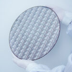
First, prioritizing planned investments towards future-ready infrastructure such as 300mm silicon and 200mm silicon carbide wafer fabs. This will enable them to reach a critical scale and maximizing the productivity and efficiency of legacy 150mm capabilities and mature 200mm capabilities.
Second, ST plans to continue to invest in upgrading the technology used across its operations, deploying additional AI and automation for additional efficiency in technology R&D, manufacturing, reliability and qualification processes, with a continued focus on sustainability.
Over the next three years, the reshaping of ST’s manufacturing footprint will design and strengthen ST’s complementary ecosystems. They are in France around digital technologies; in Italy around analog and power technologies; and in Singapore on mature technologies.
The optimization of these operations aim to achieve full capacity utilization and drive technological differentiation to compete globally. Each of ST’s current sites will continue to play a long-term role within the company’s global operations.
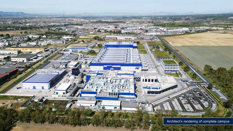
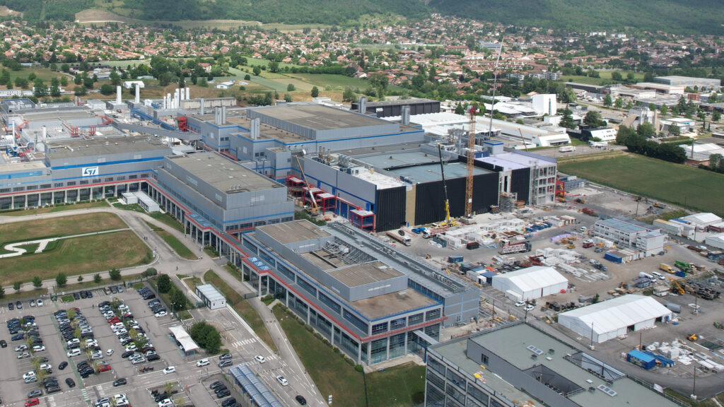
Building up 300mm Si Fabs in Agrate, Crolles
The Agrate 300mm fab in Italy will continue to be scaled up, with the aim to become ST’s flagship high-volume manufacturing facility for smart power and mixed signal technologies.
According to ST’s program, the plan is to double its current capacity to 4,000 wafers per week by 2027, with planned modular expansions increasing capacity up to 14,000 wafers per week, depending on market conditions.
As the company increases its focus on 300mm manufacturing, the Agrate 200mm fab will refocus on MEMS.
On the other hand, the Crolles 300mm fab in France will be further cemented as the core of ST’s digital products ecosystem. The plan is to increase capacity to 14,000 wafers per week by 2027 with planned modular expansions increasing capacity up to 20,000 wafers per week, depending on market conditions.
In addition, ST will convert the Crolles 200mm fab to support Electrical Wafer Sorting high volume manufacturing and advanced packaging technologies, hosting activities that do not exist today in Europe. The focus will be on next-generation leading technologies including optical sensing and silicon photonics.
Specialized Manufacturing for Power Electronics
The Catania site in Italy will continue to serve as a center of excellence for power and wide-bandgap semiconductor devices. The development of the new Silicon Carbide Campus is progressing as planned, with production of 200mm wafers set to begin in Q4 2025. Thus, reinforcing ST’s leadership in next-generation power technologies.
The company’s resources supporting Catania’s current 150mm and EWS capabilities will be refocused on 200mm silicon carbide and silicon power semiconductor production, including GaN-on-silicon, reinforcing ST’s leadership in next-generation power technologies.
Optimizing Other Manufacturing Sites
Meanwhile, ST’s Rousset line in France will remain focused on 200mm manufacturing, with additional volumes reallocated from other sites. Therefore, enabling full saturation of existing manufacturing capacity for optimized efficiency.
The Tours site also in France will remain focused on its 200mm silicon production line for select technologies, while other activities – including legacy 150mm manufacturing activities – will be transferred to different ST sites. It will also remain a center of competence for GaN, mainly on epitaxy.
The Tours site will also host a new activity: panel-level-packaging, one of the major enablers of chiplets, a technology for complex semiconductor applications that will be key for ST in the future.
Meanwhile, ST’s Ang Mo Kio site in Singapore, a high-volume fab for mature technologies, will remain focused on 200mm silicon manufacturing. Moreover, it will also host our consolidated global legacy 150mm silicon capabilities.
Lastly, the Kirkop site in Malta, ST’s high-volume test and packaging fab in Europe will be upgraded, with the addition of advanced automated technologies which will be key to support next-generation products.
12 April 2025
- Share: