ASIA ELECTRONICS INDUSTRYYOUR WINDOW TO SMART MANUFACTURING
Toray Develops Bonding Material for Ultra-Thin Wafers
Toray Industries, Inc. has developed a semiconductor back-end process material that is essential for manufacturing semiconductor wafers 30 micrometers or less in thickness. Applications for this temporary bonding material include next-generation high-bandwidth memory (HBM; see note 1) for AI semiconductors, NAND flash memory for solid-state drives, and power semiconductors for electric and electrified vehicles and industrial equipment.
The company has begun shipping samples on the new material. It plans to use its existing mass production facilities to launch volume manufacturing by 2028.
Enhances Semiconductor Performance
Global data volumes are increasing an average of 30% annually as AI and high-speed communications continue to expand. This trend makes it vital to enhance the performance of semiconductors that process such enormous amounts of data. Manufacturers need to increase the number of semiconductor chip layers while making the chips thinner to boost processing capacity. Power semiconductors must be as thin as possible to reduce energy consumption and improve response speeds.
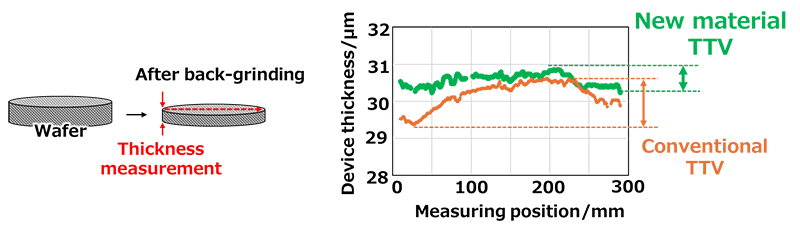
The elastic modulus of Toray’s new material is 2.5 times higher than that of its conventional counterpart. It suppresses the deformation of semiconductor process materials during back-grinding (see note 2) and evenly distributes pressure across the wafer surface. The company thus reduced the total wafer thickness variation (see note 3) after thinning to below 1.0 micrometer.
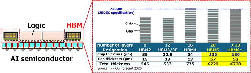
The miniaturization of transistors and wiring, which are essential for enhancing semiconductor performance in massive data processing, is reaching its physical limits. It is thus increasingly hard to improve performance by extending conventional technologies. To address this challenge, integration technology that vertically stacks multiple semiconductor chips, is emerging as a key technology to dramatically improve processing.
HBM used in AI semiconductors (see Figure 1) and NAND flash memory devices leverage this vertical integration technology to deliver superior processing performance and plays a vital role in next-generation semiconductor design.
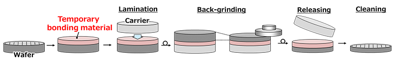
Semiconductor chips generally originate from semiconductor wafers that engineers dice in back-end processing. Manufacturers must first thin the wafers through back-grinding before dicing.
In back-grinding, engineers fix a wafer to a carrier substrate (note 4), grind it down, and then peel the thinned wafer from the substrate. This process relies on a temporary bonding material used in back-end steps (note 5).
Groundbreaking Technology
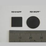
Toray develops and manufactures temporary bonding materials for semiconductors and displays using polyimide, a highly heat-resistant resin. Toray designed and developed this new material specifically for back-grinding. Using mass-produced 12-inch silicon wafers, it demonstrated that the material thins wafers to the practical limit while keeping them highly uniform (see Figures 2 and 3). The company made the material free of per- and poly-fluoroalkyl substances and N-methylpyrrolidone, which are increasingly subject to regulation because of their environmental and health concerns.
Toray will keep leveraging its core technologies of synthetic organic and polymer chemistry, biotechnology, and nanotechnology to pursue R&D into groundbreaking materials that can transform the world in keeping with its commitment to delivering new value and contributing to social progress.
Notes
- High-bandwidth memory features rapid data transfer speeds. In AI semiconductors, it plays a crucial role in rapidly supplying vast amounts of data to graphics processing units for real-time processing.
- Back-grinding is a semiconductor manufacturing process that thins wafers, and is essential to make chips smaller and create higher-density packaging.
- Total thickness variation represents the difference between the thickest and thinnest parts of a wafer.
- A carrier substrate temporarily attaches and supports a processed wafer, preventing warping or breakage, especially when thinning wafers.
- Temporary bonding material bonds a wafer to the carrier substrate, and must remain bonded during processing but enable easy peeling off afterward.
- Share: