ASIA ELECTRONICS INDUSTRYYOUR WINDOW TO SMART MANUFACTURING
Infineon Reaches 300mm SiC Manufacturing Milestone
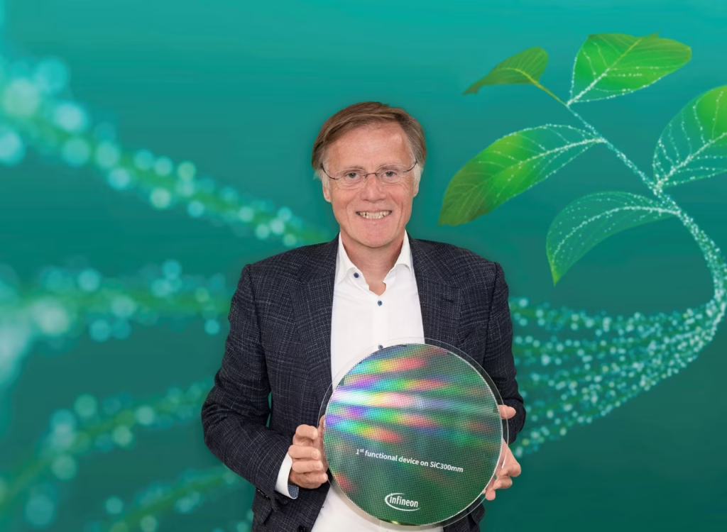
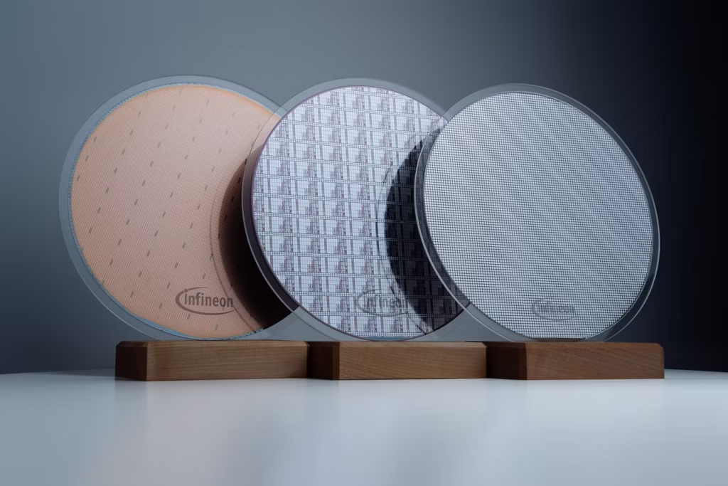
Infineon Technologies has achieved what it describes as an industry first by processing 300-millimeter silicon carbide (SiC) wafers into functional power semiconductor devices at its Villach, Austria manufacturing facility, marking a potential turning point in the future scaling of SiC production.
The milestone is strategically significant because it moves 300 mm SiC technology beyond laboratory demonstrations and into a full-scale semiconductor manufacturing environment. According to the company, the achievement was realized using existing silicon production equipment, creating a potential pathway toward more efficient and scalable SiC manufacturing.
The development comes as demand for power semiconductors continues to broaden across electric vehicles, renewable energy systems, industrial automation equipment and emerging AI data center infrastructure.
“This technological milestone further strengthens our leadership in power systems,” said Jochen Hanebeck, CEO of Infineon Technologies. “Leadership in power semiconductors means continuously pushing technology to the next level. With silicon, gallium nitride and now silicon carbide 300-millimeter wafers, we are in a leading position to scale semiconductor manufacturing and drive profitable growth.”
Increasing Manufacturing Efficiency
A key advantage of the transition to larger wafers is productivity. Infineon said 300 mm wafer production is significantly more efficient than manufacturing on 200 mm wafers because the larger substrate can accommodate approximately 2.3 times more chips per wafer.
The accomplishment provides evidence that future industrialization of 300 mm SiC technology may be technically feasible. While the company emphasized that commercialization plans and production ramp timing will be determined in collaboration with customers and partners, Infineon intends to continue executing its existing 200 mm SiC manufacturing roadmap.
Addressing Expanding Power Semiconductor Demand
The announcement also reflects the growing importance of SiC technology across high-efficiency power conversion applications. SiC devices are increasingly used in traction inverters, onboard chargers, EV charging systems, energy storage installations, industrial drives and uninterruptible power supplies.
Infineon further highlighted rising demand from AI data center infrastructure, where SiC technology is finding roles in power supply units, solid-state transformers and circuit protection systems.
The company said the new manufacturing milestone supports its objective of providing customers with a secure and cost-effective supply base for future power semiconductor requirements.
In parallel with the Villach achievement, Infineon reported that it has successfully demonstrated the feasibility of its Cold Split technology with 300 mm SiC wafers at its Dresden, Germany site. The company plans to showcase the first processed 300 mm SiC wafer publicly during the electronica trade show in Munich.
10 November 2026
- Share: