ASIA ELECTRONICS INDUSTRYYOUR WINDOW TO SMART MANUFACTURING
TSMC Launches New Alliance to Accelerate 3D IC
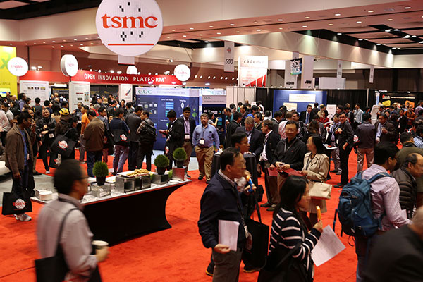
Taiwan Semiconductor Manufacturing Company Limited (TSMC) has launched the Open Innovation Platform (OIP) 3DFabric Alliance at the 2022 Open Innovation Platform Ecosystem Forum.
To illustrate, the new TSMC 3DFabric™ Alliance is TSMC’s sixth OIP Alliance and the first of its kind in the semiconductor industry. Particularly, it joins forces with partners to accelerate 3D IC ecosystem innovation and readiness, with a full spectrum of best-in-class solutions and services for semiconductor design, memory modules, substrate technology, testing, manufacturing, and packaging.
This alliance will help customers achieve speedy implementation of silicon and system-level innovations and enable next-generation HPC and mobile applications using TSMC’s 3DFabric technologies, a comprehensive family of 3D silicon stacking and advanced packaging technologies.
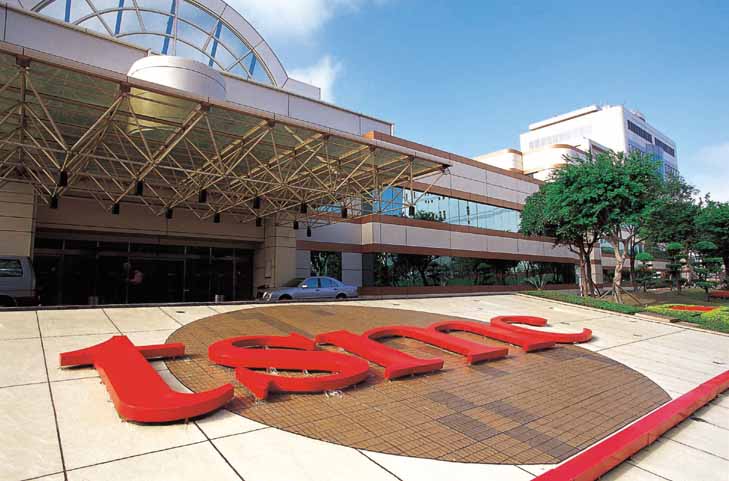
“3D silicon stacking and advanced packaging technologies open the door to a new era of chip-level and system-level innovation, and also require extensive ecosystem collaboration to help designers navigate the best path through the myriad options and approaches available to them,” said Dr. L.C. Lu, TSMC fellow and vice president of design and technology platform.
In addition, Lu said, “Through the collective leadership of TSMC and our ecosystem partners, our 3DFabric Alliance offers customers an easy and flexible way to unlocking the power of 3D IC in their designs, and we can’t wait to see the innovations they can create with our 3DFabric technologies.”
OIP 3DFabric Alliance
AMD senior vice president of technology & product engineering Mark Fuselier said, “As a pioneer in both chiplets and 3D silicon stacking, AMD is excited about the introduction of TSMC’s 3DFabric Alliance and the vital role it will play in accelerating system-level innovation.”
“We’ve already seen the benefits of working with TSMC and its OIP partners on the world’s first TSMC-SoIC™-based CPUs, and we’re looking forward to collaborating even more closely to drive the development of a robust chiplet stacking ecosystem for future generations of energy-efficient, high-performance chips.”
As the industry’s most comprehensive and vibrant ecosystem, the TSMC OIP consists of six alliances. Namely, the members are EDA Alliance, IP Alliance, Design Center Alliance (DCA), Value Chain Alliance (VCA), Cloud Alliance, and now, the 3DFabric Alliance. Furterhmore, TSMC launched OIP in 2008 to help customers overcome the rising challenges of semiconductor design complexity by creating a new paradigm of collaboration, organizing development and optimization across TSMC’s technologies, electronic design automation (EDA), IP, and design methodology.
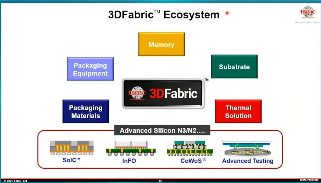
Partners of the new 3DFabric Alliance have early access to TSMC’s 3DFabric technologies, enabling them to develop and optimize their solutions in parallel with TSMC. Hence, giving customers a head start on their product development with early availability of the highest-quality, readily-available solutions and services from EDA and IP to DCA/VCA, Memory, OSAT (Outsourced Semiconductor Assembly and Test), Substrate, and Testing.
New Collaboration with 3DFabric Alliance Partners
EDA partners have early access to the TSMC 3DFabric technologies for EDA tool development and enhancement to offer optimized EDA tools and design flows to enable 3D IC designs more efficiently.
In addition, IP partners develop 3D IC IPs compliant with die-to-die interface standards and TSMC 3DFabric technologies to provide a broad variety of highest-quality, proven IP solutions for customers.
Hence, DCA/VCA partners gain early collaboration with mutual customers in 3DFabric technologies and roadmap alignment with TSMC. This will improve their service capability for 3DFabric design, IP integration, and production.
Memory partners have early technology engagement to define specs and early alignment on engineering and technical criteria with TSMC that will shorten time-to-market for future HBM generations to meet 3D IC design requirements.
OSAT partners supporting TSMC’s production quality and technical requirements collaborate with TSMC to fulfill customers’ production demands with continuous improvements in all aspects of technology and production enablement and support.
Substrate partners have early technology engagement and development with TSMC to meet future requirements of 3DFabric technologies that will improve substrate material quality, reliability, and new substrate integration to speed up production of customers’ 3D IC designs.
Testing partners have early collaboration with TSMC to develop test and stress methodologies for TSMC’s 3DFabric technologies, offering comprehensive coverage of reliability and quality requirements to help customers quickly launch their differentiated products.
“NVIDIA has been manufacturing with TSMC’s CoWoS® technologies and supporting infrastructure for several generations of high-performance GPU products,” said Joe Greco, senior vice president, advanced technology group, NVIDIA. “TSMC’s new 3DFabric Alliance will extend the technology to a broader set of products and an enhanced level of integration.”
TSMC 3Dblox™
To address the rising complexity of 3D IC design, TSMC introduced the TSMC 3Dblox™ standard to unify the design ecosystem with qualified EDA tools and flows for TSMC 3DFabric technology. The modularized TSMC 3Dblox standard is designed to model, in one format, the key physical stacking and the logical connectivity information in 3D IC designs. TSMC has worked with EDA partners in the 3DFabric alliance to enable 3Dblox for every aspect of 3D IC designs, including physical implementation, timing verification, physical verification, electro-migration IR drop (EMIR) analysis, thermal analysis, and more. TSMC 3Dblox is designed to maximize flexibility and ease of use, offering ultimate 3D IC design productivity.
TSMC 3DFabric Technologies
TSMC 3DFabric, a comprehensive family of 3D silicon stacking and advanced packaging technologies, further extends the Company’s advanced semiconductor technology offerings to unleash system-level innovations. TSMC’s 3DFabric consists of both frontend, 3D chip stacking or TSMC-SoIC™ (System on Integrated Chips), and backend technologies that include the CoWoS® and InFO family of packaging technologies, enabling better performance, power, form factor, and functionality to realize system-level integrations. In addition to CoWoS and InFO that have been in volume production, TSMC also started TSMC-SoIC silicon stacking manufacturing in 2022. TSMC now has the world’s first fully automated fab for 3DFabric in Chunan, Taiwan that integrates advanced testing, TSMC-SoIC, and InFO operations together, offering the best flexibility for customers to optimize their packaging by leveraging better cycle time and quality control.
