ASIA ELECTRONICS INDUSTRYYOUR WINDOW TO SMART MANUFACTURING
Siemens New Solution Automates 2.5D, 3DIC DFT
Siemens Digital Industries Software has introduced the Tessent™ Multi-die software solution. Accordingly, this helps customers dramatically speed and simplify critical design-for-test (DFT) tasks for ICs based on 2.5D and 3D architectures.
As demand for smaller, more power efficient and higher performing ICs continues to challenge the global IC design community. Particularly, next-generation devices increasingly feature complex 2.5D and 3D architectures that connect dies vertically (3DIC) or side-by-side (2.5D). However, these approaches can present significant challenges for IC test, since most legacy IC test approaches are based on conventional two-dimensional processes.
Optimize Manufacturing Test Cost
To address these challenges, Siemens has introduced Tessent Multi-die software. Particularly, the software is now the industry’s most comprehensive DFT automation solution for highly complex DFT tasks associated with 2.5D and 3DIC designs. The new solution works seamlessly with Siemens’ Tessent™ TestKompress™ Streaming Scan Network software and Tessent™ IJTAG software. The latter optimizes DFT test resources for each block without concern for impacts to the rest of the design. Hence, streamlining DFT planning and implementation for the 2.5D and 3DIC era.
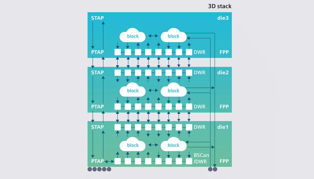
Using Tessent Multi-die software, IC design teams can rapidly generate IEEE 1838 compliant hardware featuring 2.5D and 3D IC architectures.
“IC design organizations are seeing dramatic spikes in IC test complexity due to the rapid adoption and deployment of designs featuring densely packed dies in 2.5D and 3D devices,” said Ankur Gupta, vice president and general manager of the Tessent business unit for Siemens Digital Industries Software. In addition, Gupta said, “With Siemens’ new Tessent Multi-die solution, our customers can be ready for the designs of tomorrow, while slashing test implementation effort and simultaneously optimizing manufacturing test cost today.”
Simplifies DFT Planning, Implementation
Besides supporting comprehensive test for 2.5D and 3DIC designs, the Tessent Multi-die solution can generate die-to-die interconnect patterns. In addition, it enables package-level test using the Boundary Scan Description Language (BSDL).
Furthermore, Tessent Multi-die supports integration of flexible parallel port (FPP) technology by leveraging the packetized data delivery capabilities of Siemens’ Tessent TestKompress Streaming Scan Network software. Introduced two years ago, Tessent TestKompress Streaming Scan Network decouples core-level DFT requirements from the chip-level test delivery resources. Moreover, this enables a no-compromise, bottom-up DFT flow that can dramatically simplify DFT planning and implementation, while reducing test time up to 4X.
“As the limits of traditional 2D IC design approaches become increasingly clear over time, more design teams are leveraging the power, performance, and form factor advantages that 2.5D and 3DIC architectures can deliver. But deploying these advanced schemes in new design starts without first establishing a DFT strategy that acknowledges the inherent challenges these architectures present can raise costs and undermine aggressive timelines,” said Laurie Balch, president and research director for Pedestal Research. “However, by evolving DFT technology to keep pace with the rapid adoption of multi-dimensional designs, EDA vendors can play a key role in further enabling global, mainstream adoption of 2.5D and 3D architectures.”
- Share: