ASIA ELECTRONICS INDUSTRYYOUR WINDOW TO SMART MANUFACTURING
Kioxa, Western Digital Announces New 3D Flash Memory
Demonstrating continued innovation, Kioxia Corporation and Western Digital Corp. has announced details of their newest 3D flash memory technology. Accordingly, applying advanced scaling and wafer bonding technologies, the 3D flash memory delivers exceptional capacity, performance, and reliability at a compelling cost.
Hence, this makes 3D flash memory ideal for meeting the needs of exponential data growth across a broad range of market segments.
Alper Ilkbahar, Senior Vice President of Technology & Strategy at Western Digital, said the new 3D flash memory demonstrates the benefits of the company’s strong partnership with Kioxia. Furthermore, it manifests both companies’ combined innovation leadership.
In addition, Ilkbahar said, “By working with one common R&D roadmap and continued investment in R&D, we have been able to productize this fundamental technology ahead of schedule and deliver high-performance, capital-efficient solutions.”

Capital-Efficient Solutions
Kioxia and Western Digital reduced the cost by introducing several unique processes and architectures, enabling continued lateral scaling advancements. Most importantly, this gives balance between vertical and lateral scaling produces greater capacity in a smaller die with fewer layers at an optimized cost.
The companies also developed groundbreaking CBA (CMOS directly Bonded to Array) technology, wherein each CMOS wafer and cell array wafer are manufactured separately in its optimized condition and then bonded together to deliver enhanced bit density and fast NAND I/O speed.
“Through our unique engineering partnership, we have successfully launched the eighth-generation BiCS FLASHTM with the industry’s highest1 bit density,” said Masaki Momodomi, Chief Technology Officer at Kioxia Corporation. “I am pleased that Kioxia’s sample shipments for limited customers have started. By applying CBA technology and scaling innovations, we’ve advanced our portfolio of 3D flash memory technologies for use in a range of data-centric applications including smartphones, IoT devices and data centers.”
The 218-layer 3D flash leverages 1Tb triple-level-cell (TLC) and quad-level-cell (QLC) with four planes and features innovative lateral shrink technology to increase bit density by over 50 percent. Moreover, its high-speed NAND I/O at over 3.2Gb/s, a 60 percent improvement over the previous generation, combined with a 20 percent write performance and read latency improvement, will accelerate overall performance and usability for users.
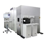
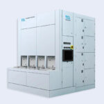
Advanced IC Manufacturing Facility
Last year Kioxia and Western Digital have celebrated the opening of the state-of-the-art semiconductor fabrication facility at the Yokkaichi Plant in Mie Prefecture, Japan. Accordingly, the production capacity at Fab7 will ramp up in stages over time, in line with market trends.
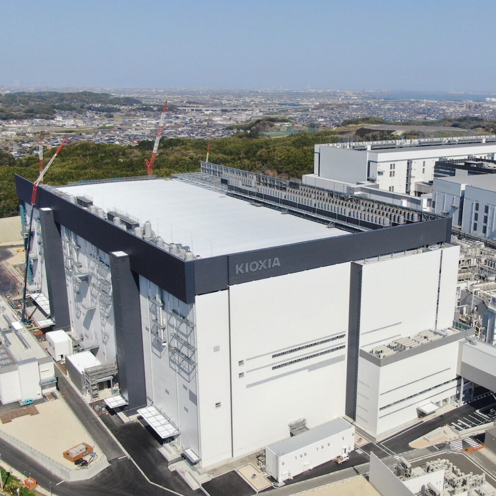
Fab7 has the capability to produce sixth-generation, 162-layer flash memory and future advanced 3D flash memory. The facility will start shipping 162-layer flash memory in early 2023.
To illustrate, the facility uses artificial intelligence for enhanced production efficiencies and employs a space-efficient facility design that enlarges the space available for manufacturing equipment in its clean rooms. Hence, the Fab7 offers safety and sustainability, capable of absorbing earthquake shocks. At the same time, it implements the latest energy-saving manufacturing equipment.
- Share: