ASIA ELECTRONICS INDUSTRYYOUR WINDOW TO SMART MANUFACTURING
USI Develops Advanced Failure Analysis Technology for SiP Miniaturization Products
Driven by 5G, consumer electronics, automotive electronics, and innovative smart applications, new packaging technologies represented by SiP are gradually emerging. The high-reliability components and semiconductor markets are experiencing explosive growth in demand for high-density, miniaturized products. To meet these advanced processes, material, and packaging applications and developments, USI develops advanced electronic component Failure Analysis (FA) technology to meet the increasingly complex and diverse needs of SiP miniaturized products.

The general failure analysis procedure consists of three key steps: confirming the failure mode, analyzing the failure mechanism, and verifying the failure mechanism and root cause. After these steps, proposing improvement actions follow. The importance of failure analysis in the integrated circuit industry chain is increasing. It is necessary to rely on more advanced and precise equipment and technology by rational failure analysis to improve the success rate of failure analysis.
To minimize process issues, USI utilizes a high-resolution 3D X-Ray to locate the position of abnormal components. It uses laser layer removal and re-ball technology to extract the main chip in the SiP module. Meanwhile, USI uses X-ray photoelectron spectroscopy (XPS) and Fourier-transform infrared spectroscopy (FTIR) to identify the source of organic contaminants on the component’s surface, continuously strengthening its capabilities in the SiP module failure analysis field.
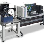
X-ray inspection does not damage the tested object so, it is considered an essential non-destructive FA technology in analyzing failure points of SiP packaged components. In addition to observing defects inside the SiP package or substrate, it can also inspect the internal structure of various components. USI has introduced high-resolution nano-level 3D X-Ray, which uses a rotating sample to obtain two-dimensional X-ray tomography images of different orientations in space. It combines these images into a three-dimensional X-ray tomography image through computer algorithms.
As the chip size and pitch of solder balls continue to shrink, traditional chemical decapsulation and direct chip extraction can cause damage to some chips’ redistribution layer (RDL) and insulation layer. USI’s R&D personnel have solved the problem of extracting and completing chip testing from the SiP module without damaging the original state of the chip through a series of methods, including finely grinding the back of the chip, laser cutting around the chip, ball mounting with a high-precision laser ball mounting machine, and cross-validating chip performance.
Due to chemical composition changes on the surface or micro-region of components or chips caused by pollution oxidation, corrosion, migration, processes, and environment, there are numerous failures. Therefore, in-situ analysis of micro-region composition is crucial. In addition to energy dispersive spectroscopy (EDS) used in conjunction with scanning electron microscopy (SEM), USI has introduced high-sensitivity analysis facilities such as XPS and FTIR.
Specifically, XPS performs elemental and chemical state analysis and measures longitudinal concentration distributions of elements from the surface to the interior with the help of ion beam sputtering, analyzing the thickness of oxide or pollution layers and the concentration distribution of dopants. Meanwhile, FTIR mainly analyzes the composition and content of organic and semiconductor materials that absorb infrared. The infrared spectra with a microscope can perform micro-region analysis with thickness at the micron level, effectively tracking the origin of organic contaminants and determining the problem’s root cause.
Robbie Tong, the Director of the New Product Development Department of USI, said, “With the continuous development of new electronic materials, new types of components, and advanced packaging processes for high-end chips, the technology and capabilities of failure analysis must keep pace with the times. Through the continuous exploration of researchers, the SiP module failure analysis method of USI has gradually become mature and continuously improved various detection and analysis technologies have played a key role in improving product quality and reducing losses from defective products.”
- Share: